Method for manufacturing organic electronic device and method for manufacturing sealing member

A technology of organic electronic components and manufacturing methods, applied in the direction of electrical components, electrical solid devices, final product manufacturing, etc., can solve problems such as damage to electronic components, and achieve the effect of suppressing the reduction of reliability and component performance

Inactive Publication Date: 2018-05-11
SUMITOMO CHEM CO LTD
View PDF10 Cites 0 Cited by
  • Summary
  • Abstract
  • Description
  • Claims
  • Application Information

AI Technical Summary

Problems solved by technology

Outgassing and UV rays m...

Method used


Image

  • Method for manufacturing organic electronic device and method for manufacturing sealing member
  • Method for manufacturing organic electronic device and method for manufacturing sealing member
  • Method for manufacturing organic electronic device and method for manufacturing sealing member

Examples


Embodiment Construction

[0035] Hereinafter, a preferred embodiment of the present invention will be described in detail with reference to the drawings. It should be noted that in the description of the drawings, the same symbols are used for the same or equivalent elements, and repeated descriptions are omitted.

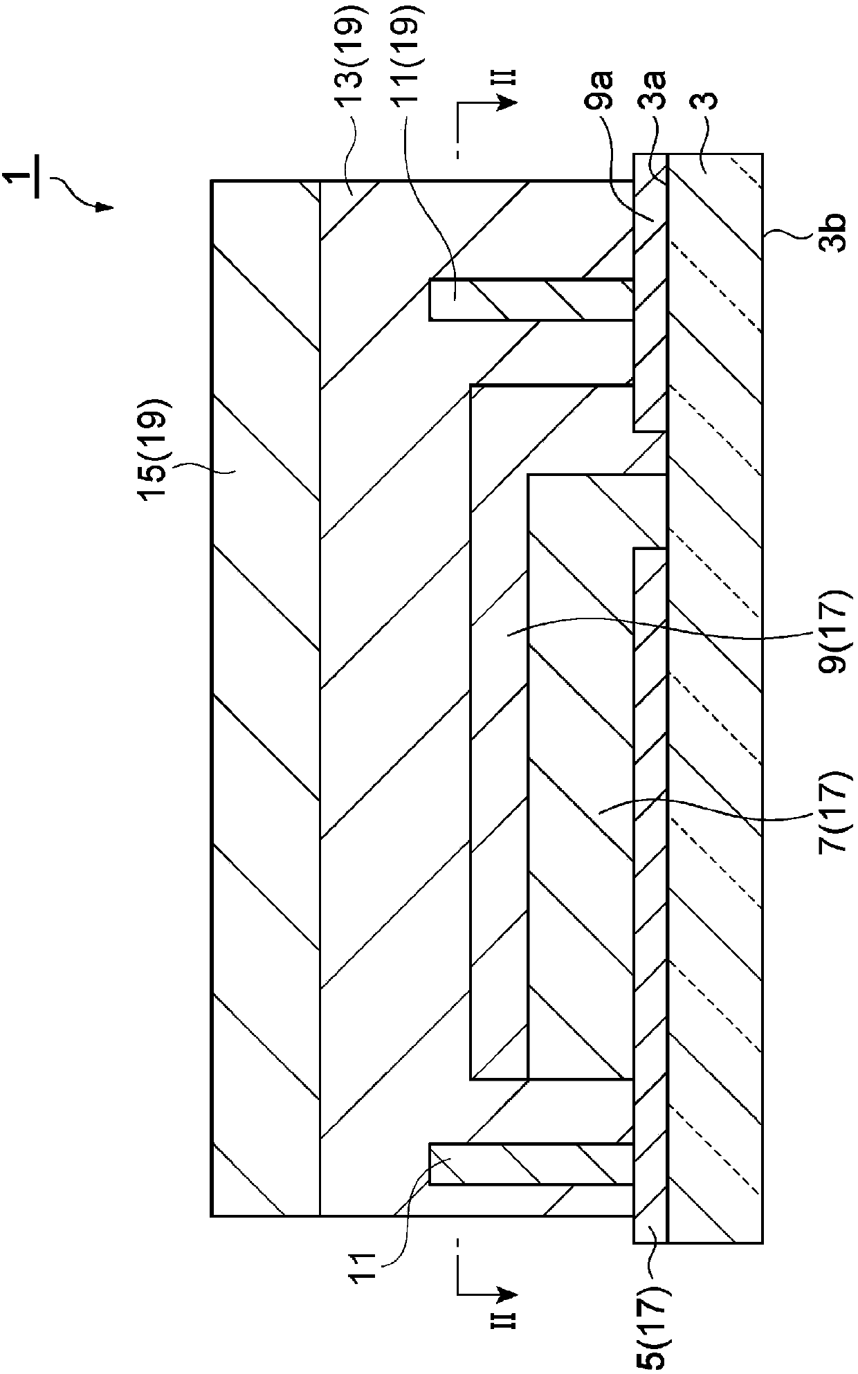
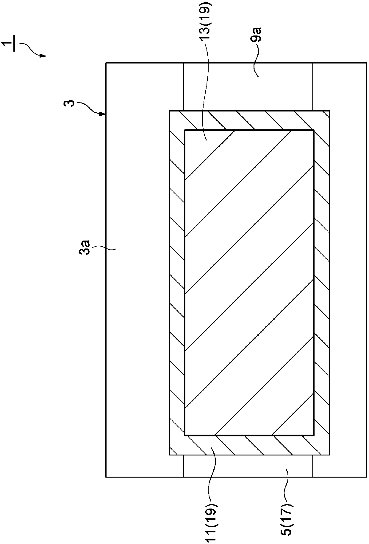
[0036] Such as figure 1 As shown, the organic EL element (organic electronic device) 1 manufactured by the method of manufacturing the organic EL element of the present embodiment includes: a support substrate 3, an anode layer 5, a light emitting layer (organic functional layer) 7, a cathode layer 9, and a moisture absorption part 11. Adhere the adhesive part 13 and the sealing substrate 15. The anode layer 5, the light-emitting layer 7, and the cathode layer 9 constitute an organic EL portion (organic electronic element) 17. The moisture absorption part 11, the adhesive bonding part 13 and the sealing substrate 15 constitute a sealing member 19.

[0037] [Support substrate]

[0038] The suppo...


PUM


Abstract

A method for manufacturing an organic electronic device in which a sealing member 19 having a sealing substrate 15, an adhesive part 13 which exhibits adhesiveness and which is provided on the sealingsubstrate 15, and a hygroscopic part 11 which is a hygroscopic cured product provided on the adhesive part 13, are affixed to an organic electronic element 17.

Description

Technical field [0001] The present invention relates to a method of manufacturing an organic electronic device and a method of manufacturing a sealing member. Background technique [0002] As a conventional manufacturing method of an organic electronic device, there is, for example, a method described in Patent Document 1. The method of manufacturing an organic electronic device described in Patent Document 1 is a method of manufacturing an electronic device having a substrate and electronic components formed on the substrate, and includes: obtaining a sealing member in which an insulating layer and an adhesive layer are formed on a sealing substrate The process, the process of forming the insulating layer removal part on the insulating layer and the adhesive layer, the process of filling the insulating removal part with the resin containing the moisture absorbent, the process of sticking the sealing member to the electronic component, and the process of bonding the sealing subst...

Claims


Application Information

Patent Timeline
IPC IPC(8): H05B33/10H01L51/50H05B33/04
CPCH05B33/04H05B33/10Y02E10/549Y02P70/50H10K50/8426H10K50/846H10K71/00H10K50/00H10K50/81H10K50/82H10K77/111
Inventor 赤对真人下河原匡哉森岛进一
Owner SUMITOMO CHEM CO LTD
Why Eureka
Try Eureka