Novel thermistor array chip and preparation method of same

A thermistor, a new type of technology, applied in the field of new thermistor chip and its preparation, can solve the problems of difficult to reduce the size of the application module, occupy a large space, unfavorable integration, etc., to improve reliability and consistency, Ease of implementation, improved installation efficiency and installation density

Inactive Publication Date: 2018-05-15
ZHAOQING EXSENSE ELECTRONICS TECH
View PDF5 Cites 4 Cited by
  • Summary
  • Abstract
  • Description
  • Claims
  • Application Information

AI Technical Summary

Problems solved by technology

However, if figure 1 As shown, the existing NTC thermistor chips generally have a single-resistor structure, and only one electrode layer 2' is provided on both sides of the thermal ceramic chip 1'. When assembling a complex circuit module, multiple NTC thermal resistors need to be mounted. When using resistor chips, it is necessary to repeatedly mount individual NTC thermistor chips on the PCB one by one for bonding. This mounting method consumes a lot of time, and at the same time, figure 2 As shown, multiple chips occupy a large space after bonding and wiring, and the installation density is low. It is difficult to reduce the size of the application module, which is not conducive to the improvement of integration.

Method used


Image

  • Novel thermistor array chip and preparation method of same
  • Novel thermistor array chip and preparation method of same
  • Novel thermistor array chip and preparation method of same

Examples


Embodiment Construction

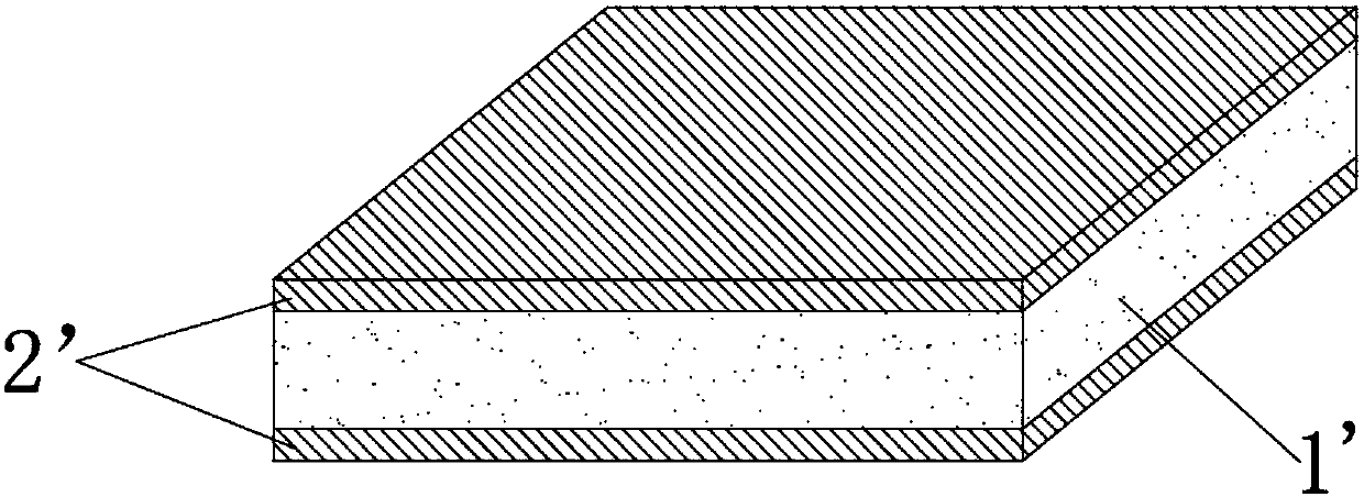
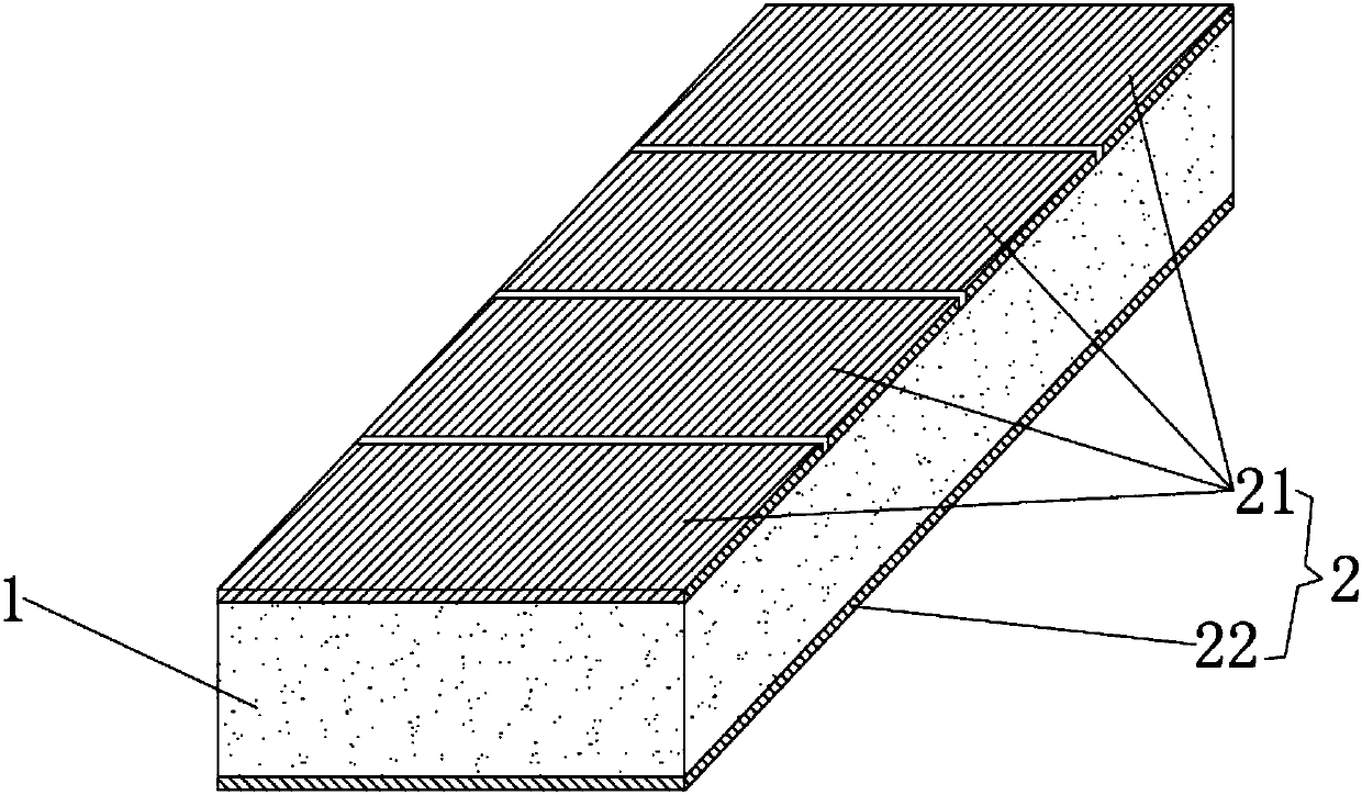
[0033] see image 3 , which is a structural diagram of the novel thermistor array chip of the present invention. The novel thermistor array chip includes a thermal ceramic chip 1 and a metal electrode 2 arranged on the surface of the thermal ceramic chip 1 .

[0034] Specifically, the heat-sensitive tile 1 is rectangular, with a thickness of 200-2000 μm, and its material is NTC heat-sensitive ceramic material.

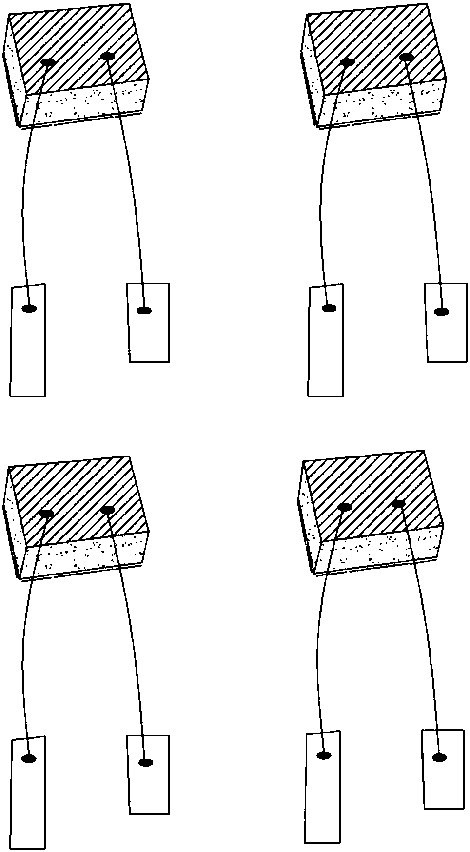
[0035] The metal electrode 2 includes at least two top electrodes 21 , preferably four top electrodes 21 in total, and one bottom electrode 22 .

[0036] The four top electrodes 21 are arranged side by side and at intervals on the upper surface of the heat-sensitive ceramic chip 1, each top electrode 21 is a rectangular layered structure, and its pair of sides is respectively connected to two sides of the heat-sensitive ceramic chip 1. The long sides are flush.

[0037] The bottom electrode 22 is a layered structure, which completely covers the lower surface of the ...


PUM

PropertyMeasurementUnit
thicknessaaaaaaaaaa
electrical resistivityaaaaaaaaaa

Abstract

The invention relates to a novel thermistor array chip which includes a thermosensitive ceramic chip and metal electrodes arranged on the surface thereof. The metal electrodes include at least two topelectrodes and one bottom electrode, wherein the top electrodes are arranged in parallel at interval on the upper surface of the thermosensitive ceramic chip. The bottom electrode completely covers the lower surface of the thermosensitive ceramic chip. The invention also relates to a preparation method of the novel thermistor array chip, which includes the steps of: press-shaping and sintering NTC thermosensitive ceramic powder to obtain a ceramic ingot, cutting the ceramic ingot into thermosensitive ceramic substrates; printing the thermosensitive ceramic substrates with a metal electrode layer, sintering the thermosensitive ceramic substrates, and cutting the thermosensitive ceramic substrates to prepare single novel thermistor array chip. The thermistor array chip is improved in installation efficiency and installation density, has flexible installation modes, has simple structure and can save circuit space and increase integration degree.

Description

technical field [0001] The invention belongs to the technical field of electronic components, in particular to a novel thermistor array chip and a preparation method thereof. Background technique [0002] NTC thermistor is an important temperature sensing element, widely used in temperature detection of household appliances, new energy vehicle battery control and temperature detection, temperature detection and temperature compensation of office automation equipment, industrial, medical, environmental protection, meteorology, food processing equipment Temperature control and detection, as well as instrument coils, temperature compensation of thermocouples, etc. [0003] COB (Chip on Board), also known as direct chip mounting technology, refers to directly pasting the bare chip on the PCB board through adhesive or solder, and then performing wire bonding to realize the electrical interconnection between the chip and the PCB board, and then The technology of encapsulating chi...

Claims


Application Information

Patent Timeline
Patent Type & Authority Applications(China)
IPC IPC(8): H01C7/04H01C17/06
CPCH01C7/04H01C17/06
Inventor 张慧敏段兆祥叶建开杨俊柏琪星唐黎民
Owner ZHAOQING EXSENSE ELECTRONICS TECH
Why Eureka
Try Eureka