Method of setting scanning threshold based on circuit design figure

A circuit design and graphics technology, applied in circuits, calculations, electrical components, etc., can solve problems that affect the judgment of current station defect results, and there are many defect signals at the previous station, so as to reduce the rate of unreal defects and improve the detection and recovery. The effect of the probability of detection

Active Publication Date: 2018-05-15
SHANGHAI HUALI MICROELECTRONICS CORP
View PDF4 Cites 2 Cited by
  • Summary
  • Abstract
  • Description
  • Claims
  • Application Information

AI Technical Summary

Problems solved by technology

However, when the signal of the current station is very large and has a high degree of similarity with the defect signal of the current station, it is difficult for some existing defect program establishment methods to filter the defect signal caused by the defect of the previous station while retaining the defect of the current station
As a result, there are too many defect signals of the previous station that engineers do not care about in the scanning results, which affects the judgment of the defect results of the current station

Method used


Image

  • Method of setting scanning threshold based on circuit design figure
  • Method of setting scanning threshold based on circuit design figure

Examples


Embodiment Construction

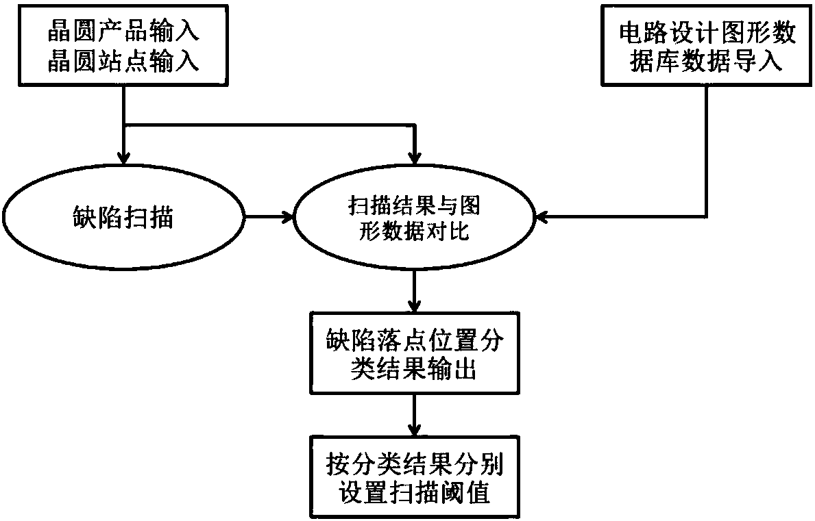
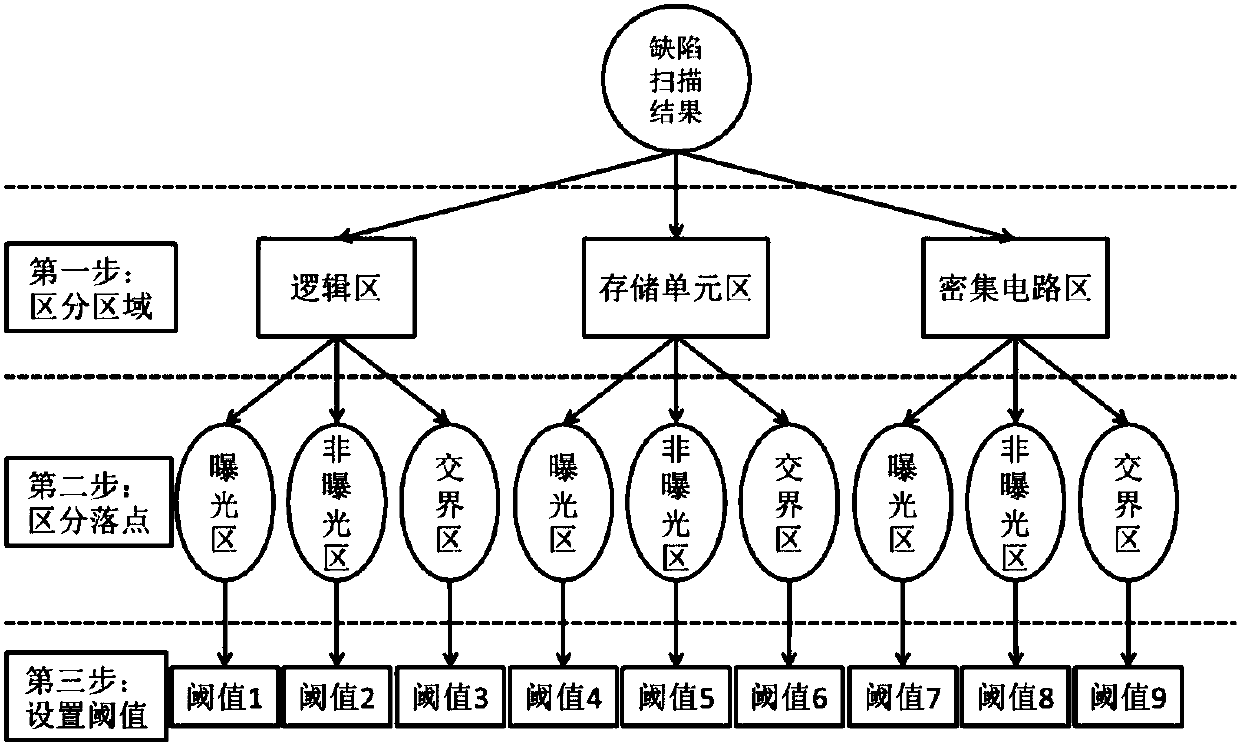
[0011] combine figure 2 As shown, the existing method for setting the scanning threshold is as follows: the first step is to divide the defects according to the scanning area, and the second step is to set the scanning threshold parameters. In the method adopted by the present invention, in the first step, defects are divided according to the scanning area, and then a step of defect classification is added. In the second step, defects are divided according to the location of the defect in the circuit design graphic. In the third step, the scanning threshold parameter is set.

[0012] The method for setting the scanning threshold according to the circuit design graph is to add a processing module including a circuit design graph database in the optical detection machine. The processing module divides the position of the defect signal point by comparing the digital gray-scale image obtained by the scanning part with the circuit design graphic of the same size as the coordinates...


PUM


Abstract

The invention discloses a method of setting a scanning threshold based on a circuit design figure. A processing module containing a circuit design figure database is added to an optical detection stock; through comparing a digital grayscale image obtained by a scanning part and a circuit design figure of the coordinate size of the extracted digital grayscale image in the circuit design figure database, the module divides a falling position of a defect signal point; and after scanning, the defect signal points obtained through scanning are divided to three different types according to falling at an exposure position, falling at non-exposure positions and falling at junction positions between exposure and non-exposure, and scanning threshold parameters are set respectively. The number of signals with front-station defects in scanning can be reduced, and the non-real defect rate of defect scanning is thus reduced.

Description

technical field [0001] The invention relates to the field of inspecting and analyzing defects on a complete wafer during the research and development of an integrated circuit manufacturing process, in particular to a method for setting a scanning threshold according to a circuit design graphic. Background technique [0002] Each site in the semiconductor manufacturing process needs to scan and detect wafer surface defects through optical inspection machines. [0003] During the defect inspection process, engineers are usually only concerned with the surface of the wafer on which it is standing. However, since the optical inspection machine uses ultraviolet light beams to detect the surface of the wafer, and at the same time, there are many kinds of films in silicon-based semiconductor wafers that have greater light transmittance to ultraviolet light beams, such as silicon dioxide, etc. , so that when the optical inspection machine is used to inspect the wafers on each stati...

Claims


Application Information

Patent Timeline
Patent Type & Authority Applications(China)
IPC IPC(8): H01L21/66G06T7/00G06T7/136
CPCG06T7/0004G06T7/136G06T2207/30148H01L22/12
Inventor 陈超郭贤权许向辉陈昊瑜
Owner SHANGHAI HUALI MICROELECTRONICS CORP
Why Eureka
Try Eureka