Manufacturing process of circuit board metallized half hole

A metallized half-hole and manufacturing process technology, which is applied to the formation of electrical connection of printing components, etc., can solve the problems of scrapping scrap, weak welding feet, and virtual welding, etc., to achieve stable product quality, improve production efficiency, and reduce production costs. Effect

Inactive Publication Date: 2018-05-15
TIGERBUILDER CIRCUIT SUZHOU
View PDF6 Cites 5 Cited by
  • Summary
  • Abstract
  • Description
  • Claims
  • Application Information

AI Technical Summary

Problems solved by technology

In this situation, when the SMT manufacturer is soldering, it will lead to weak soldering feet and virtual soldering, which will seriously cause a bridge short circuit between the two pins.
Therefore, most PCB manufacturers use manual repair as a solution, which is inefficient and prone to scrapping and scrapping

Method used


Image

  • Manufacturing process of circuit board metallized half hole
  • Manufacturing process of circuit board metallized half hole

Examples


Embodiment Construction

[0038] The following will clearly and completely describe the technical solutions in the embodiments of the present invention with reference to the accompanying drawings in the embodiments of the present invention. Obviously, the described embodiments are only some, not all, embodiments of the present invention. Based on the embodiments of the present invention, all other embodiments obtained by persons of ordinary skill in the art without making creative efforts belong to the protection scope of the present invention.

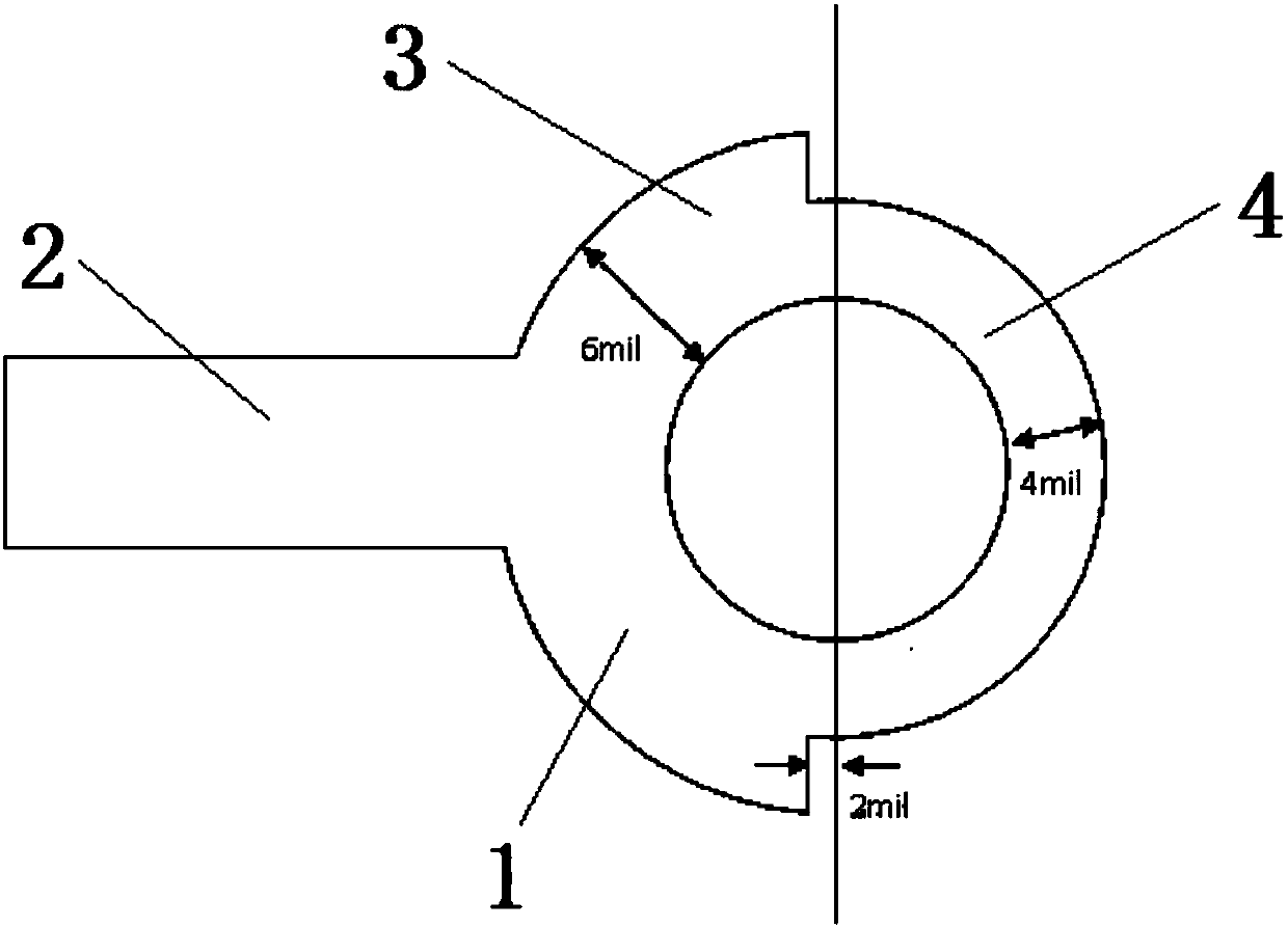
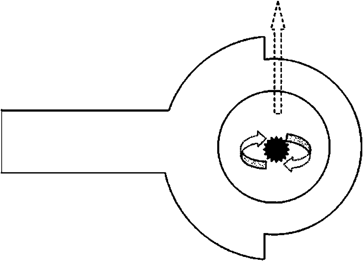
[0039] Such as Figure 1 to Figure 2 Shown, for the manufacturing process of a kind of circuit board metallization half-hole 1 of the present invention, comprise the steps:

[0040] S1: Preprocess and obtain multilayer boards, the front and back of the multilayer boards are bare copper surfaces;

[0041] S2: Make outer layer circuit patterns on the front and back sides of the multilayer board, the outer layer circuit patterns include reserved metallized half ...


PUM


Abstract

The invention discloses a manufacturing process of a circuit board metallized half hole. The manufacturing process includes the following steps: S1, preprocessing and acquiring a multi-layer board, wherein the front surface and the back surface of the multi-layer board are light copper surfaces; S2, manufacturing an outer-layer circuit pattern on the front surface and the back surface of the multi-layer board, wherein the outer-layer circuit pattern comprises a reserved metallized half hole; S3, printing the protective ink on the position where the metallized half hole needs to be manufacturedby means of a screen printer, wherein the protective ink needs to completely cover the ring of the metallized half hole; S4, milling the metallized half hole in the position where the metallized halfhole is manufactured; S5, washing the protective ink by using a fading ink; S6, brushing off the metal burrs generated during rotary cutting of a milling cutter by using a deburring machine; S7, spraying emery to the board by a sand blasting machine at a high speed, further removing burrs, so that the surface is smooth and flat; and S8, carrying out the subsequent processing. The method effectively solves the industrial general technical problems of the tilting and coming off of the ring and the residual copper wire burrs in the hole when the metallized half hole circuit board is produced.

Description

technical field [0001] The invention relates to the technical field of circuit board preparation, in particular to a process for manufacturing metallized half holes of a circuit board. Background technique [0002] In recent years, with the rapid development of electronic products, high density, multi-function, and miniaturization have become the development direction. Nowadays, the size of circuit boards continues to decrease, and customers often need to match some small carrier boards. The characteristics of these small carrier boards are: the individual is relatively small, and there is a whole row of metallized half-holes on the side of the unit. As a daughter board of a motherboard, these metallized half-holes are welded together with the motherboard and the pins of components. [0003] At present, the production process of circuit boards has two processes: additive method (including semi-additive method) and subtractive method. The metallized half-hole circuit board ...

Claims


Application Information

Patent Timeline
Patent Type & Authority Applications(China)
IPC IPC(8): H05K3/42
Inventor 陈斌刘国强熊力徐艳
Owner TIGERBUILDER CIRCUIT SUZHOU
Why Eureka
Try Eureka