Self-aligning dual mesa device structure making method

A technology of device structure and fabrication method, applied in the fields of semiconductor/solid-state device manufacturing, semiconductor devices, electrical components, etc., can solve the problems of affecting the consistency between chips, reducing the process yield, wasting chip area, etc., and achieving accurate diameter and size Controllable, improve tape-out efficiency and reduce device cost

Inactive Publication Date: 2018-05-18
INST OF ELECTRONICS ENG CHINA ACAD OF ENG PHYSICS
View PDF3 Cites 4 Cited by
  • Summary
  • Abstract
  • Description
  • Claims
  • Application Information

AI Technical Summary

Problems solved by technology

[0005] 1. The photolithography registration step is introduced, and the registration error of each film is different, which reduces the process yield and also affects the chip consistency
The registration error of the two overlays makes the small table deviate from the center of the large table. If the registration error is large, the small table will be close to the side of the large table, and the device structure will fail.
[0006] 2. There is a secondary etching problem
In the second step of photolithography and etching, a small mesa is formed, but the large mesa in the first step is etched twice, and the effective depth of the large mesa is not easy to control
Considering that the diameter of the small mesa is the effective area of ​​the device, although the double-mesa structure can improve the performance of the device, it greatly reduces the duty cycle of the focal plane device array and wastes the chip area.

Method used


Image

  • Self-aligning dual mesa device structure making method
  • Self-aligning dual mesa device structure making method
  • Self-aligning dual mesa device structure making method

Examples


Embodiment Construction

[0031] In order to further illustrate the technical means and effects adopted by the present invention to achieve the predetermined invention objectives, the specific implementation manners of the present invention will be described below in conjunction with examples of the invention.

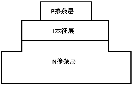
[0032] Select PIN structure GaN material, such as figure 2 shown. An implementation mode corresponding to the fabrication method of the self-aligned double-mesa device structure of the present invention is as follows:

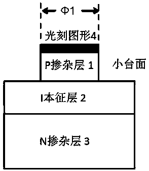
[0033] Step 1, prepare a small mesa photolithographic pattern 4 on the P-doped layer, such as image 3 shown.

[0034] The photoresist used in the implementation is AZ4620, and the photoresist spin-coating condition is: 2000 revolutions, 30 seconds. After pre-baking at 100°C for 150 seconds, photolithographic exposure for 40 seconds, and developing with a developer for 2 minutes, a small mesa photolithographic pattern 4 is formed. The obtained photolithographic pattern 4 ha...


PUM


Abstract

The invention relates to a self-aligning dual mesa device structure making method. Based on the photoresist reflow process, one-step photolithography is used to make a dual mesa device structure, anddual mesa center self-aligning is carried out. The method is advantaged in that one step of lithography is omitted, flow sheet efficiency is improved, flow sheet cost is reduced, the edge interval between a large mesa and a small mesa can be smaller than 1um and can be further adjusted through photoresist reflow technology control, and the method is especially suitable for making a focal plane array with the high duty ratio.

Description

technical field [0001] The invention belongs to the application field of semiconductor photoelectric devices, and in particular relates to a method for manufacturing a self-aligned double-mesa device structure. Background technique [0002] Wide bandgap semiconductor materials are widely used in optoelectronic devices in the ultraviolet band, and typical materials include GaN, SiC, ZnO, etc. The APD (Avalanche Photodiode) photodetector device prepared by using the avalanche breakdown effect of wide bandgap materials has extremely high avalanche gain, can detect weak ultraviolet light or even ultraviolet single photons, and is widely used in environmental monitoring, medical equipment and other fields. [0003] The APD device structure based on wide-bandgap materials is generally a mesa structure, and mesa sidewall absorption recombination leakage and edge breakdown are prone to occur during high-field avalanche. In order to achieve a high avalanche gain above 10^5, the lite...

Claims


Application Information

Patent Timeline
Patent Type & Authority Applications(China)
IPC IPC(8): H01L31/18H01L21/027H01L21/68
CPCH01L21/0274H01L21/68H01L31/1856Y02P70/50
Inventor 王旺平李沫李倩康健彬张健
Owner INST OF ELECTRONICS ENG CHINA ACAD OF ENG PHYSICS
Why Eureka
Try Eureka