Manufacture method for improving solder resist hole plugging ink seepage

A manufacturing method and hole plugging technology, which are applied in printed circuit manufacturing, secondary processing of printed circuits, electrical components, etc., can solve the problems of removal, low production efficiency, and high processing costs, and improve production efficiency, production efficiency, and processing. Time-saving effect

Inactive Publication Date: 2018-05-18
KIN YIP TECHNOLDGY ELECTRONICS HUI ZHOUCO LTD
View PDF3 Cites 9 Cited by
  • Summary
  • Abstract
  • Description
  • Claims
  • Application Information

AI Technical Summary

Problems solved by technology

The commonly used method of solder mask plugging is to expose the hole first and then perform solder mask treatment on the board surface. The problem with this processing method is that oil explosion will occur during post-baking and cause the solder mask to sputter onto the pad.
At present, the commonly used processing method of solder mask plug hole is to use two times of solder mask, that is, first solder mask the plug hole, solidify the solder mask in the through hole and then silk screen the surface solder mask, the first solder mask only plugs the hole, and then Solder resistance on the surface of the circuit board. The process flow of this processing method is: pre-process → board electricity → outer layer graphics → graphic plating → outer layer etching → outer layer AOI → plug hole before solder mask → solder mask → next process, Among them, the process flow of the plug hole before solder mask is: pre-treatment of solder mask → solder mask plug hole → pre-baking → exposure (with exposure film) → development → post-baking → pre-treatment of solder mask → silk screen surface solder mask → pre-baking →Exposure→Post-baking, the defects of this processing method are that the oil explosion problem will occur during the post-baking process of the plug hole before the solder mask, which will cause the solder mask to sputter onto the pad, the process is long and the production efficiency is low, and the processing The cost is high, and this processing method cannot remove the solder resist sputtered onto the pad, so that the solder resist remains on the processed circuit board, and there are defects of oil leakage at the solder resist plug hole

Method used


Image

  • Manufacture method for improving solder resist hole plugging ink seepage

Examples


Embodiment

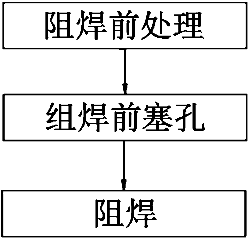
[0020] Example: such as figure 1 As shown, the present invention provides a method for improving oil spillage in solder resist plug holes, comprising the steps of:

[0021] 1) Solder mask pre-treatment: pre-baking plate treatment before solder mask pre-treatment, specifically, the baking plate treatment specifically includes: when the holes to be plugged on the circuit board include back-drilled holes, before the solder mask pre-treatment step Perform pre-baking plate treatment, and / or, perform post-baking plate treatment after the pre-treatment step of solder mask; when the hole to be plugged on the circuit board is a through hole with a high thickness-to-diameter ratio, perform post-baking after the pre-treatment step of solder mask Board treatment, when performing pre-baking board treatment, keep the temperature of 150°C±5°C for 60min-120min; when performing post-baking board treatment, keep the temperature of 75°C±5°C for 10min-30min; then remove the through hole oxides, ...


PUM


Abstract

The invention discloses a manufacture method for improving solder resist hole plugging oil seepage. The method comprises the following steps of: pre-solder resist procedure treatment; pre-solder resist procedure hole plugging; and solder resist treatment. According to the manufacture method of the invention, board baking treatment is additionally adopted, and therefore, residual moisture left in the holes and base materials of a circuit board can be removed, the defect of ink seepage which appears after the solder resist hole plugging and solidification of the circuit board are performed can be effectively eliminated, the quality of a product can be improved, time consumed by solder resist hole plugging and solder resist treatment is shortened, production efficiency can be improved; an abrasive belt is adopted to perform board grinding treatment, so that solder resist can be prevented from sputtering to hole plugging ink on the circuit board during the pre-solder resist procedure holeplugging, and therefore, it can be ensured that a circuit formed during the formation process of an outer-layer pattern will not be damaged; a negative film for solder resist exposure is improved, evenly distributed light sensing points are added on blocking points on the double-side-windowed negative film which are used for solder resist hole plugging, and therefore, the solder resist in throughholes can be exposed to a certain extent; and under the same development condition, the technical procedures of the solder resist in the through holes are decreased compared with those of the ink on the surface of the circuit board, and production efficiency is improved.

Description

technical field [0001] The invention relates to the technical field of circuit board manufacturing, in particular to a method for improving the oil spillage of solder resist plug holes. Background technique [0002] In the process of circuit board processing, plug holes are often designed on the circuit board in order to prevent soldering tin flow, and for heat dissipation considerations, copper surfaces are usually designed to form double-sided window plug holes. The solder resist plug hole with double-sided windows is a through hole on the circuit board, and the through hole needs to be filled with solder resist, while the annular ring of the double-sided through hole needs to be windowed instead of solder resist. The commonly used method of plugging the solder mask is to expose the hole first and then perform the solder mask treatment on the board surface. The problem with this processing method is that oil explosion will occur during post-baking and cause the solder mask...

Claims


Application Information

Patent Timeline
Patent Type & Authority Applications(China)
IPC IPC(8): H05K3/00H05K3/22H05K3/28
Inventor 刘小军田成友
Owner KIN YIP TECHNOLDGY ELECTRONICS HUI ZHOUCO LTD
Why Eureka
Try Eureka