Exposure apparatus, exposure method, and method of manufacturing article
A technology of exposure device and optical path, which is applied in the direction of exposure device of photolithography process, microlithography exposure equipment, photoplate process of pattern surface, etc., can solve the problems such as difficult to accurately align the substrate, and achieve the effect of precise alignment
- Summary
- Abstract
- Description
- Claims
- Application Information
AI Technical Summary
Problems solved by technology
Method used
Image

Examples
no. 1 example
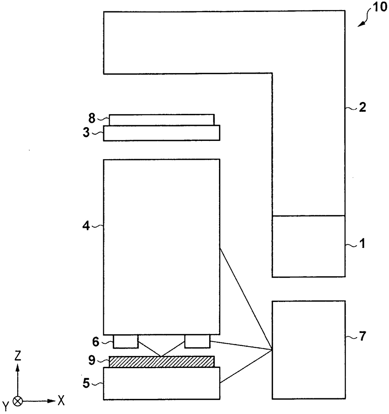
[0023] will refer to figure 1 An exposure apparatus 10 according to a first embodiment of the present invention is described. figure 1 is a schematic diagram showing the exposure apparatus 10 according to the first embodiment. The exposure apparatus 10 according to the first embodiment may include, for example, a light source 1 , an illumination optical system 2 , a mask stage 3 , a projection optical system 4 , a substrate stage 5 , a measurement unit 6 , and a control unit 7 . The control unit 7 includes, for example, a CPU and a memory, and controls each unit of the exposure device 10 (controls the operation of exposing the irradiated area of the substrate 9 ). Also, in the present embodiment, a direction parallel to the optical axis of light emitted from the projection optical system 4 is set as the Z direction, and two directions perpendicular to the optical axis and orthogonal to each other are set as the X direction. direction and the Y direction.
[0024] For exam...
PUM
 Abstract
Description
Claims
Application Information
 - Generate Ideas
- Intellectual Property
- Life Sciences
- Materials
- Tech Scout
- Unparalleled Data Quality
- Higher Quality Content
- 60% Fewer Hallucinations
Browse by: Latest US Patents, China's latest patents, Technical Efficacy Thesaurus, Application Domain, Technology Topic, Popular Technical Reports.
© 2025 PatSnap. All rights reserved.Legal|Privacy policy|Modern Slavery Act Transparency Statement|Sitemap|About US| Contact US: help@patsnap.com