

Scintillation ceramic array and preparation method thereof
A technology of scintillation ceramics and arrays, applied in scintillation elements, measuring devices, instruments, etc., can solve the problems of low light output, low reflectivity of the side glue of a single die, X-ray crosstalk, etc., to reduce penetration, improve Light output performance, improve the effect of reflection
- Summary
- Abstract
- Description
- Claims
- Application Information
AI Technical Summary
Problems solved by technology
Method used
Image

Examples
Embodiment 1
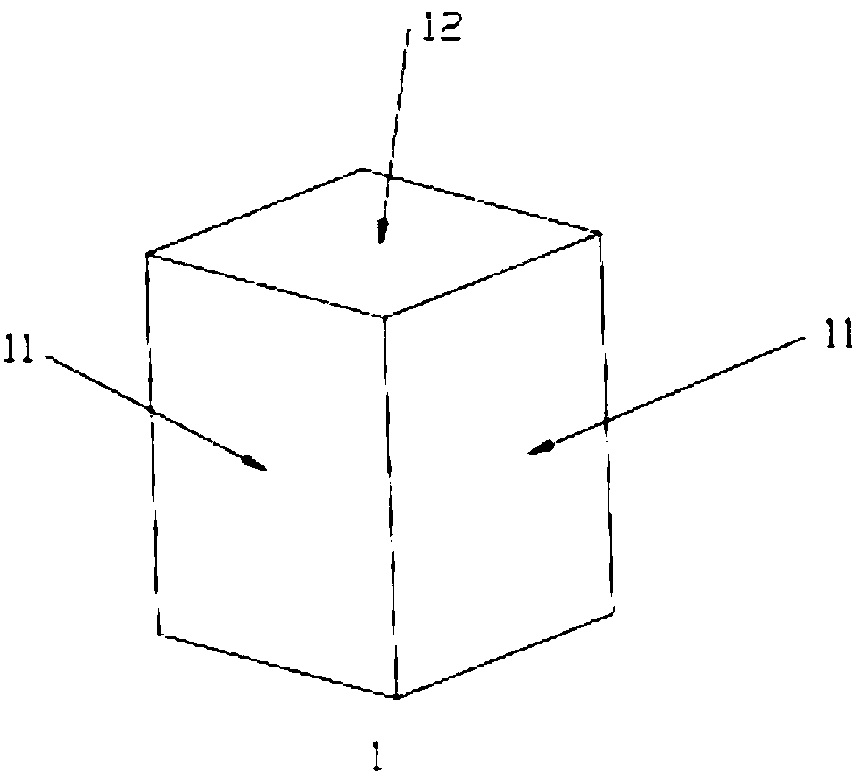
[0028] Ceramic scintillator Ce 0.005 (Lu 0.1 Y 0.9 ) 2.995 (Al 0.4 Ga 0.6 ) 5 o 12 As a basic element, the Ag metal reflective layer with a thickness of 0.01mm is plated on the side, and the epoxy resin reflective layer with a thickness of 0.5mm is plated on the top surface.
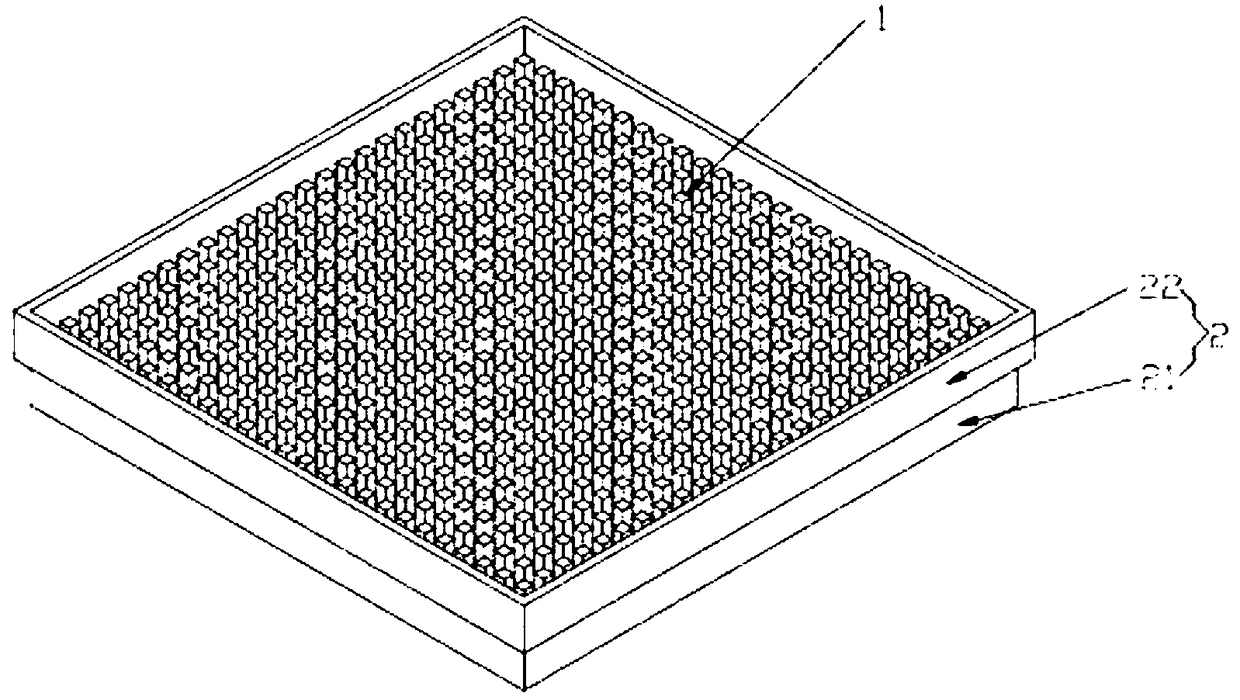
[0029] The preparation method is as follows: the ceramic material of the basic element is cut into single cuboid crystal grains by mechanical processing method, the side of the crystal grain is plated with Ag with a thickness of 0.01 mm by chemical deposition method, and the Ag reflective layer is plated on multiple sides. The scintillator primitives are respectively arranged into an array structure by using combined screening plates, and then imported as figure 2 In the positioning coupling mold shown, epoxy resin with reflective medium is poured into the gaps between multiple scintillator elements, and finally cured, and the epoxy resin on the top surface is ground to 0.5mm, and the bottom ligh...
Embodiment 2
[0031] Ceramic scintillator Ce 0.005 (Lu 0.1 Y 0.9 ) 2.995 (Al 0.4 Ga 0.6 ) 5 o 12 As a basic unit, the Ag metal reflective layer with a thickness of 0.05mm is plated on the side, and the epoxy resin reflective layer with a thickness of 0.5mm is plated on the top surface.
[0032] The preparation method is as follows: the ceramic material of the element is cut into single cuboid crystal grains by mechanical processing method, the side of the crystal grain is plated with Ag with a thickness of 0.05 mm by chemical deposition method, and the Ag reflective layer is plated on multiple sides. The scintillator primitives are respectively arranged into an array structure by using combined screening plates, and then imported as figure 2 In the positioning coupling mold shown, epoxy resin with reflective medium is poured into the gaps between multiple scintillator elements, and finally cured, and the epoxy resin on the top surface is ground to 0.5mm, and the bottom light-emittin...
Embodiment 3
[0034] Ceramic scintillator Eu 0.015 (Lu 0.1 Gd 0.9 ) 3.3 (Al 0.6 sc 0.4 ) 4.685 o 12 As a primitive, the side is coated with a Pt metal reflective layer with a thickness of 0.05mm, and the top is coated with a 0.5mm epoxy resin reflective layer.
[0035] Its preparation method is as follows: the ceramic material of the basic element is cut into single cuboid crystal grains by mechanical processing method, 0.05mm of Pt is plated on the sides of the crystal grains by chemical deposition method, and multiple sides are plated with Pt of the same thickness to reflect The scintillators of each layer are arranged into an array structure by using combined screening plates, and then imported into figure 2 In the positioning coupling mold shown, the epoxy resin with reflective medium is poured into the gaps between multiple scintillator elements, and finally cured, the top epoxy resin is ground to 0.5mm, and the bottom light-emitting surface is polished. Polish to obtain the d...
PUM
| Property | Measurement | Unit |
|---|---|---|
| Thickness | aaaaa | aaaaa |
Abstract
Description
Claims
Application Information