Silicon wafer inserting device, silicon wafer cleaning equipment and silicon wafer cleaning method

A technology for silicon wafer insertion and silicon wafer cleaning, applied in transportation and packaging, conveyor objects, sustainable manufacturing/processing, etc., can solve the problems of poor cleaning effect and prolong cleaning time, so as to improve cleaning efficiency and reduce Cleaning time, the effect of improving efficiency

Pending Publication Date: 2018-06-01
LONGI GREEN ENERGY TECH CO LTD
View PDF9 Cites 3 Cited by
  • Summary
  • Abstract
  • Description
  • Claims
  • Application Information

AI Technical Summary

Problems solved by technology

[0004] The object of the present invention is to provide a silicon wafer inserting device, which solves the problem that the cleaning effect is not good due to the too close distance between two adjacent silicon wafers when the existing silicon wafer is inserted.
[0005] The purpose of the present invention is also to provide a silicon wafer cleaning equipment, which solves the shortcoming that the existing silicon wafer cleaning equipment needs to prolong the cleaning time because the distance between the silicon wafers is too close

Method used


Image

  • Silicon wafer inserting device, silicon wafer cleaning equipment and silicon wafer cleaning method
  • Silicon wafer inserting device, silicon wafer cleaning equipment and silicon wafer cleaning method

Examples


Embodiment Construction

[0027] The present invention will be described in detail below in conjunction with the accompanying drawings and specific embodiments.

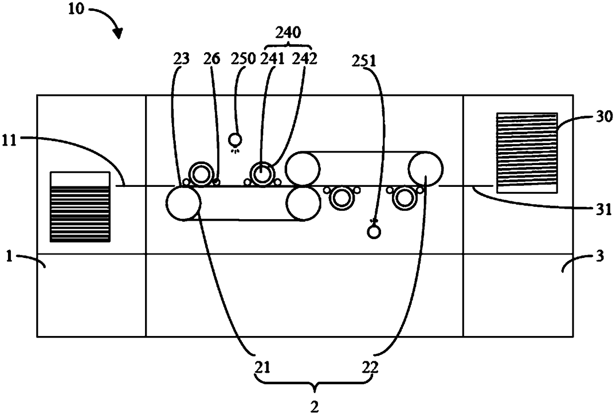
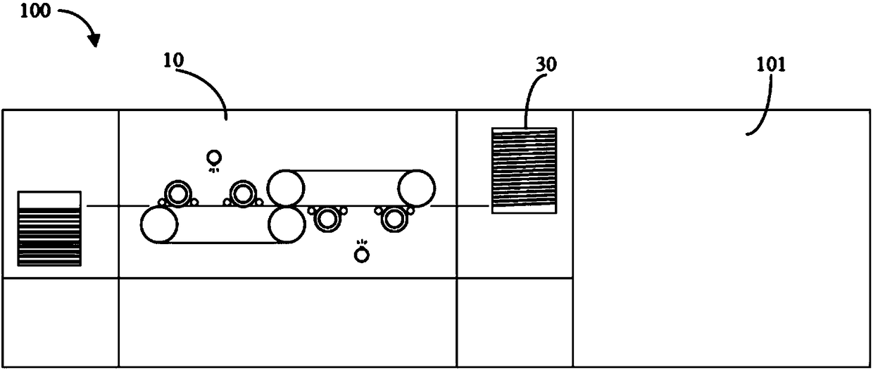
[0028] see figure 1 , The first embodiment of the present invention provides a silicon wafer inserting device 10 , including a loading unit 1 , a cleaning unit 2 and a wafer inserting unit 3 which are connected. The feeding unit 1 transfers the silicon wafers to the inserting unit 3 one by one. The cleaning unit 2 is located between the loading unit 1 and the insertion unit 3 , and cleans the silicon wafers before entering the insertion unit 3 .

[0029] The feeding unit 1 has a feeding conveying unit 11 communicating with the cleaning unit 2 . The loading unit 1 can be a loading structure in the prior art, and the silicon wafers are transferred to the loading and conveying unit 11 one by one.

[0030] The cleaning unit 2 includes at least one cleaning section. Specifically, the cleaning unit 2 may include a plurality of cleaning sections ...


PUM


Abstract

The invention provides a silicon wafer inserting device, which comprises a feeding unit and an inserting unit which communicate with each other, wherein the feeding unit is used for transmitting silicon wafers to the inserting unit one by one; the silicon wafer inserting device also comprises a cleaning unit located between the feeding unit and the inserting unit; and the cleaning unit is used forcarrying out cleaning treatment on the silicon wafers before entering the inserting unit. Silicon wafer cleaning equipment comprises a silicon wafer cleaning device and the silicon wafer inserting device. According to a silicon wafer cleaning method, cleaning is carried out by using the silicon wafer cleaning equipment, and the silicon wafer cleaning method comprises the steps of transmitting thesilicon wafers by using the feeding unit; cleaning the silicon wafers by using the cleaning unit; transmitting the silicon wafers subjected to cleaning treatment to the inserting unit for inserting;and cleaning the inserted silicon wafers by using the silicon wafer cleaning device. According to the silicon wafer inserting device, the silicon wafer cleaning equipment and the silicon wafer cleaning method, the silicon wafers before entering the inserting unit are subjected to cleaning treatment by using the cleaning unit, so that dirt on the surface is reduced and the standing time of the silicon wafers in a cleaning tank can be greatly shortened.

Description

technical field [0001] The invention belongs to the technical field of solar cell manufacturing, and in particular relates to a silicon wafer insertion device, a silicon wafer cleaning device with the silicon wafer insertion device, and a silicon wafer cleaning method. Background technique [0002] With the continuous development of the world economy, the demand for high-efficiency energy in modernization is increasing. Photovoltaic power generation, as a green energy source and a major energy source for the sustainable development of human beings, has been increasingly valued by countries all over the world and has been vigorously developed. Cells with silicon wafers as the main body are mainstream products in the field of solar cells, and the required silicon wafers are obtained by slicing square or quasi-square silicon ingots or silicon rods. The multiple silicon wafers obtained by slicing are stacked together, and need to be sliced ​​and inserted. The multiple silicon w...

Claims


Application Information

Patent Timeline
Patent Type & Authority Applications(China)
IPC IPC(8): H01L21/67H01L21/677H01L31/18
CPCH01L31/18H01L21/67011H01L21/67017H01L21/677Y02P70/50
Inventor 魏超锋郭江涛邓浩张济蕾曹明奇梁刚
Owner LONGI GREEN ENERGY TECH CO LTD
Why Eureka
Try Eureka