Superimposed three-dimensional transistor and its manufacturing method

A transistor and three-dimensional technology, applied in semiconductor/solid-state device manufacturing, semiconductor devices, electrical components, etc., can solve the problems of occupying space, high cost of semiconductor chips, unfavorable integration of semiconductor chip devices, etc., to improve device integration and reduce overall cost effect

Active Publication Date: 2021-06-11
SHENZHEN MYD INFORMATION TECH CO LTD
View PDF6 Cites 0 Cited by
  • Summary
  • Abstract
  • Description
  • Claims
  • Application Information

AI Technical Summary

Problems solved by technology

Since the fins are formed vertically on the silicon substrate, they need to occupy a certain space, which is not conducive to improving the device integration of semiconductor chips.
Therefore, generally speaking, the cost of semiconductor chips using the above-mentioned fin field effect transistors is relatively high.

Method used


Image

  • Superimposed three-dimensional transistor and its manufacturing method
  • Superimposed three-dimensional transistor and its manufacturing method
  • Superimposed three-dimensional transistor and its manufacturing method

Examples


Embodiment Construction

[0019] The following will clearly and completely describe the technical solutions in the embodiments of the present invention. Obviously, the described embodiments are only some of the embodiments of the present invention, rather than all the embodiments. Based on the embodiments of the present invention, all other embodiments obtained by persons of ordinary skill in the art without making creative efforts belong to the protection scope of the present invention.

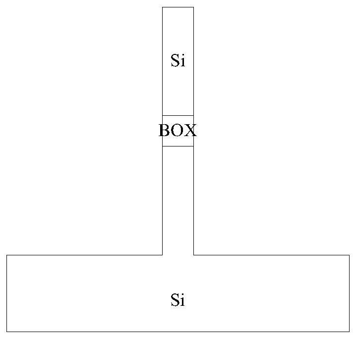
[0020] In order to solve the problems of low device integration and high cost in the existing three-dimensional field effect transistors, the present invention provides a method for manufacturing a superimposed three-dimensional transistor and a superimposed three-dimensional transistor manufactured by the above-mentioned method. By etching the buried oxide layer of the SOI substrate, the semiconductor materials above and below the buried oxide layer of the SOI substrate are used as the channel regions of the two thre...


PUM


Abstract

The present invention provides a method for manufacturing a superimposed three-dimensional transistor, comprising: providing an SOI substrate, the SOI substrate comprising a back substrate, a buried oxide layer and a top layer silicon; and etching the SOI substrate to form a superimposed fin structure; An insulating material is formed on the back substrate, the insulating material surrounds the stacked fin structure; the insulating material is etched, so that the stacked fin structure is exposed and formed on the surface of the back substrate an insulating layer; forming a gate dielectric layer on the surface of the stacked fin structure; forming a gate around the gate dielectric layer. The present invention also provides a stacked three-dimensional transistor fabricated according to the above fabrication method. The superimposed three-dimensional transistor and the manufacturing method thereof of the present invention can improve the device integration degree of the semiconductor chip and effectively reduce the cost.

Description

【Technical field】 [0001] The invention relates to the technical field of semiconductor chip manufacturing, in particular to a stacked three-dimensional transistor and a manufacturing method thereof. 【Background technique】 [0002] A Fin Field Effect Transistor (FinFET) is a field effect transistor with a fin-shaped channel structure. In a fin field effect transistor, a fin (Fin) is vertically formed on the surface of a silicon substrate, and the fin serves as a channel, and a gate (gate) controls the channel by covering the surface of the fin. In the working process of the fin field effect transistor, the carriers flow from the source to the drain, and the gate is located between the source and the drain. In fact, the fin using the above-mentioned fin channel structure The field effect transistor is a three-dimensional field effect transistor. Since the fins are vertically formed on the silicon substrate, they need to occupy a certain space, which is not conducive to impro...

Claims


Application Information

Patent Timeline
Patent Type & Authority Patents(China)
IPC IPC(8): H01L21/822H01L21/8234
CPCH01L21/8221H01L21/823431H01L29/785
Inventor 不公告发明人
Owner SHENZHEN MYD INFORMATION TECH CO LTD
Why Eureka
Try Eureka