Novel GaN-based LED device structure

A technology for LED devices and device structures, applied in semiconductor devices, electrical components, circuits, etc., can solve the problems of heat accumulation, complicated processes, and high excitation temperature, and achieve the effect of extending service life, improving heat dissipation efficiency, and high device integration.

Inactive Publication Date: 2018-06-01
XIAN ZHISHENG RUIXIN SEMICON TECH CO LTD
View PDF0 Cites 0 Cited by
  • Summary
  • Abstract
  • Description
  • Claims
  • Application Information

AI Technical Summary

Problems solved by technology

Among them, the packaging method in which the phosphor powder is evenly distributed in the packaging material is easy to operate, but the excitation efficiency of the phosphor powder in this packaging method is low; because the phosphor powder is far away from the chip, the process is complicated and difficult to control. Industrial production has not yet been realized; the phosphor powder is close to the chip. The packaging method is to bond the chip with the help of an intermediary packaging material. The defect is that the refractive index of the intermediary packaging material is low, and the light emitted by the chip is prone to total reflection, resulting in heat accumulation, which reduces the light output efficiency of the chip and affects the excitation of phosphors. (The excitation temperature of the phosphor is relatively high)
Applying phosphor powder directly to the semi-finished product that has been bonded to the die will cause a lot of waste of phosphor powder

Method used


Image

  • Novel GaN-based LED device structure
  • Novel GaN-based LED device structure
  • Novel GaN-based LED device structure

Examples


Embodiment 1

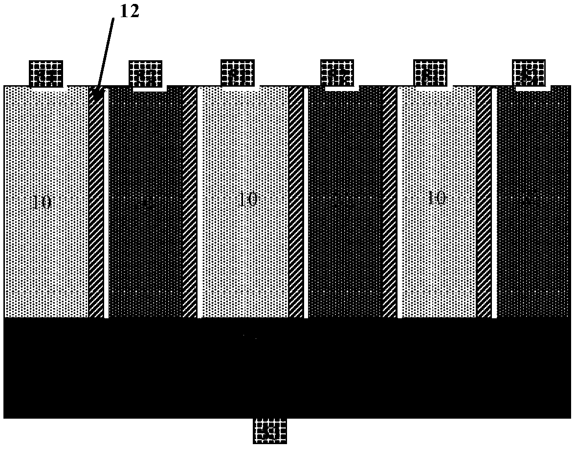
[0041] See figure 1 , figure 1 It is a schematic structural diagram of a novel GaN-based LED device provided by an embodiment of the present invention. The device structure includes:

[0042] conductive substrate 410;

[0043] A reflective layer 40, disposed on the conductive substrate 410;

[0044] The metal electrode layer 407 is disposed on the reflective layer 40;

[0045] A plurality of GaN blue light epitaxial layers 10 and a plurality of GaN ultraviolet light epitaxial layers 20 are arranged at intervals in sequence on the metal electrode layer;

[0046] The first cathode electrode 51 is disposed on the GaN blue light epitaxial layer 10;

[0047] The second cathode electrode 52 is disposed on the GaN ultraviolet epitaxial layer 20;

[0048] The anode electrode 53 is disposed under the conductive substrate 410 .

[0049] Wherein, the conductive substrate 410 is a doped Si sheet, an aluminum sheet or a copper sheet.

[0050] Wherein, the GaN blue light epitaxial l...

Embodiment 2

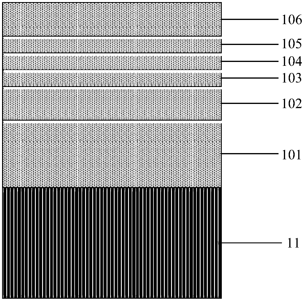
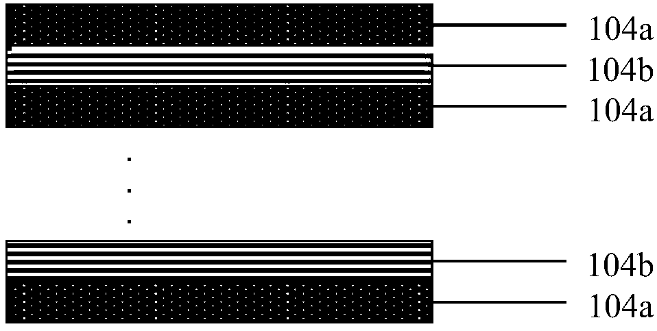
[0060] See Figure 2 to Figure 9 , figure 2 A schematic diagram of the growth of a GaN blue light epitaxial layer provided by the embodiment of the present invention; image 3 A schematic diagram of the growth of a first active layer provided by an embodiment of the present invention; Figure 4 A schematic diagram of the preparation of an ultraviolet light wick groove provided by an embodiment of the present invention; Figure 5 A schematic diagram of the growth of a GaN ultraviolet epitaxial layer provided by the embodiment of the present invention; Figure 6 A schematic diagram of the growth of a second active layer provided by an embodiment of the present invention; Figure 7 A schematic diagram of the preparation of a conductive substrate provided by an embodiment of the present invention; Figure 8 A schematic top view of an electrode fabrication provided by an embodiment of the present invention; Figure 9 It is a schematic cross-sectional view of an electrode fabr...


PUM

PropertyMeasurementUnit
Thicknessaaaaaaaaaa
Thicknessaaaaaaaaaa
Thicknessaaaaaaaaaa

Abstract

The invention relates to a novel GaN-based LED device structure. The structure comprises a conductive substrate; a reflection layer which is disposed on the conductive substrate; a metal electrode layer which is disposed on the reflection layer; a plurality of blue-light epitaxial layers and a plurality of GaN ultraviolet-light epitaxial layers, which are all sequentially arranged on the metal electrode layer at intervals; a first negative electrode which is disposed on the blue-light epitaxial layers; a second negative electrode which is disposed on the GaN ultraviolet-light epitaxial layers;and a positive electrode which is disposed below the conductive substrate. According to the invention, a GaN epitaxial wafer is transferred to a substrate material with the good electrical and thermal conduction characteristics from a sapphire substrate, so the structure can improve the heat dissipation efficiency, and prolongs the service life of a device.

Description

technical field [0001] The invention relates to the technical field of integrated circuits, in particular to a novel GaN-based LED device structure. Background technique [0002] LED (Lighting Emitting Diode) is a light-emitting diode, which is a semiconductor solid-state light-emitting device. It uses a solid semiconductor chip as a light-emitting material. In the semiconductor, the excess energy is released through the recombination of carriers to cause photon emission, which directly emits red, yellow, blue, and green light. LED is a new type of solid-state light source, which has many advantages such as small size, high luminous efficiency, low energy consumption, long life, no mercury pollution, all solid state, fast response, low working voltage, safety and reliability. [0003] Utilizing the principle of three primary colors, phosphor powder can be added in the packaging of LED devices to emit light of any color, so LEDs can be used as light sources for lighting. In...

Claims


Application Information

Patent Timeline
IPC IPC(8): H01L33/32H01L33/06H01L33/46H01L33/36
CPCH01L33/32H01L33/06H01L33/36H01L33/46
Inventor 张捷
Owner XIAN ZHISHENG RUIXIN SEMICON TECH CO LTD
Why Eureka
Try Eureka