Fabrication method of novel GaN-based LED

A new type of blue-light material technology, applied in electrical components, circuits, semiconductor devices, etc., can solve the problems of phosphor waste, complicated process, and high excitation temperature, and achieve the effects of reducing production costs, flexible luminous colors, and high device integration

Inactive Publication Date: 2018-06-08
XIAN ZHISHENG RUIXIN SEMICON TECH CO LTD
View PDF0 Cites 0 Cited by
  • Summary
  • Abstract
  • Description
  • Claims
  • Application Information

AI Technical Summary

Problems solved by technology

Among them, the packaging method in which the phosphor powder is evenly distributed in the packaging material is easy to operate, but the excitation efficiency of the phosphor powder in this packaging method is low; because the phosphor powder is far away from the chip, the process is complicated and difficult to control. Industrial production has not yet been realized; the phosphor powder is close to the chip. The packaging method is to bond the chip with the help of an intermediary packaging material. The defect is that the refractive index of the intermediary packaging material is low, and the light emitted by the chip is prone to total reflection, resulting in heat accumulation, which reduces the light output efficiency of the chip and affects the excitation of phosphors. (The excitation temperature of the phosphor is relatively high)
Applying phosphor powder directly to the semi-finished product that has been bonded to the die will cause a lot of waste of phosphor powder

Method used


Image

  • Fabrication method of novel GaN-based LED
  • Fabrication method of novel GaN-based LED
  • Fabrication method of novel GaN-based LED

Examples


Embodiment 1

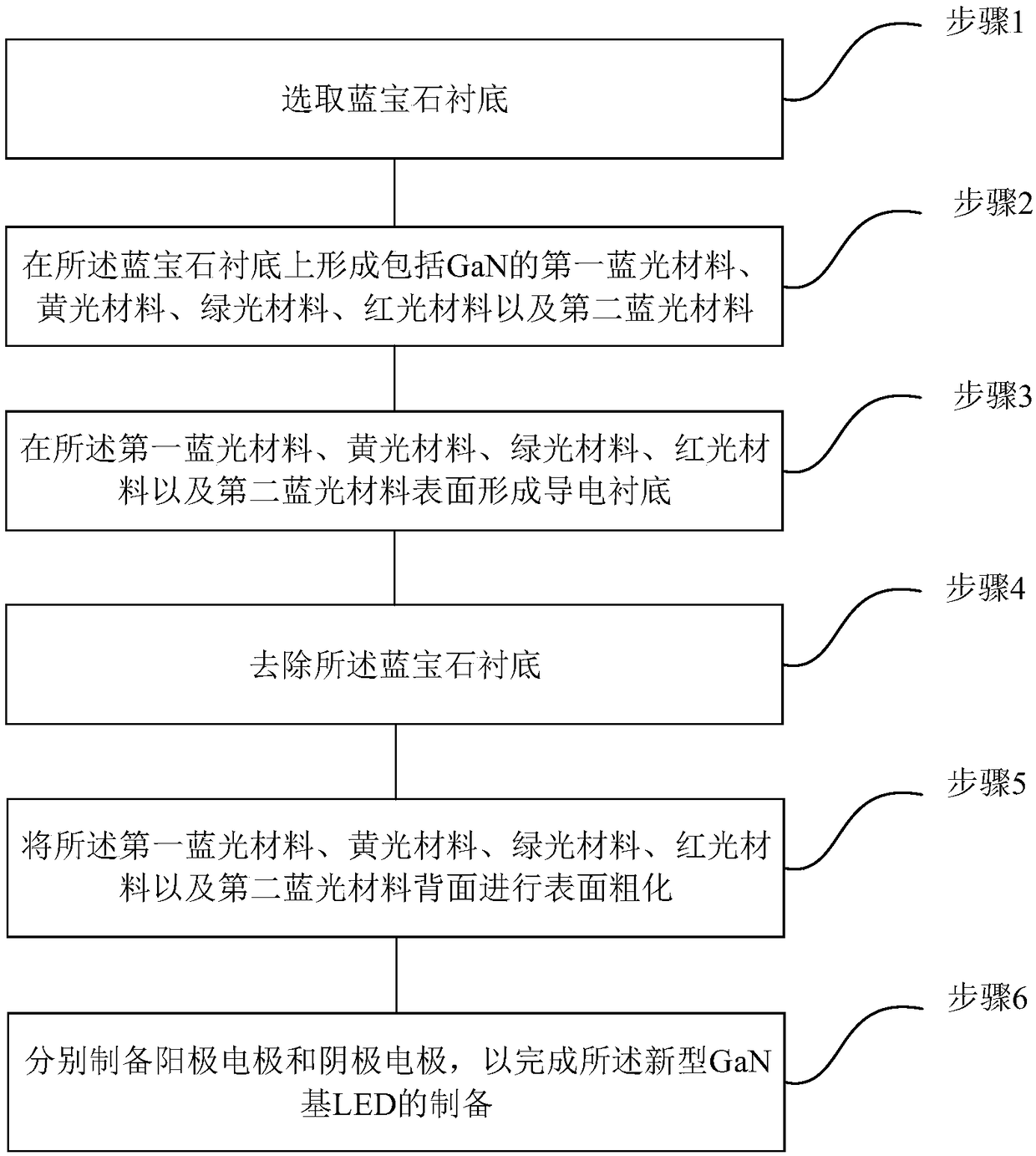
[0060] See figure 1 , figure 1 A flow chart of a novel GaN-based LED manufacturing method provided by an embodiment of the present invention. This preparation method comprises the steps:

[0061] Step 1, select the sapphire substrate;

[0062] Step 2, forming a first blue light material, a yellow light material, a green light material, a red light material and a second blue light material including GaN on the sapphire substrate;

[0063] Step 3, forming a conductive substrate on the surface of the first blue light material, yellow light material, green light material, red light material and second blue light material;

[0064] Step 4, removing the sapphire substrate;

[0065] Step 5, roughening the back surface of the first blue light material, yellow light material, green light material, red light material and second blue light material;

[0066] Step 6. Prepare the anode electrode and the cathode electrode respectively, so as to complete the preparation of the novel GaN...

Embodiment 2

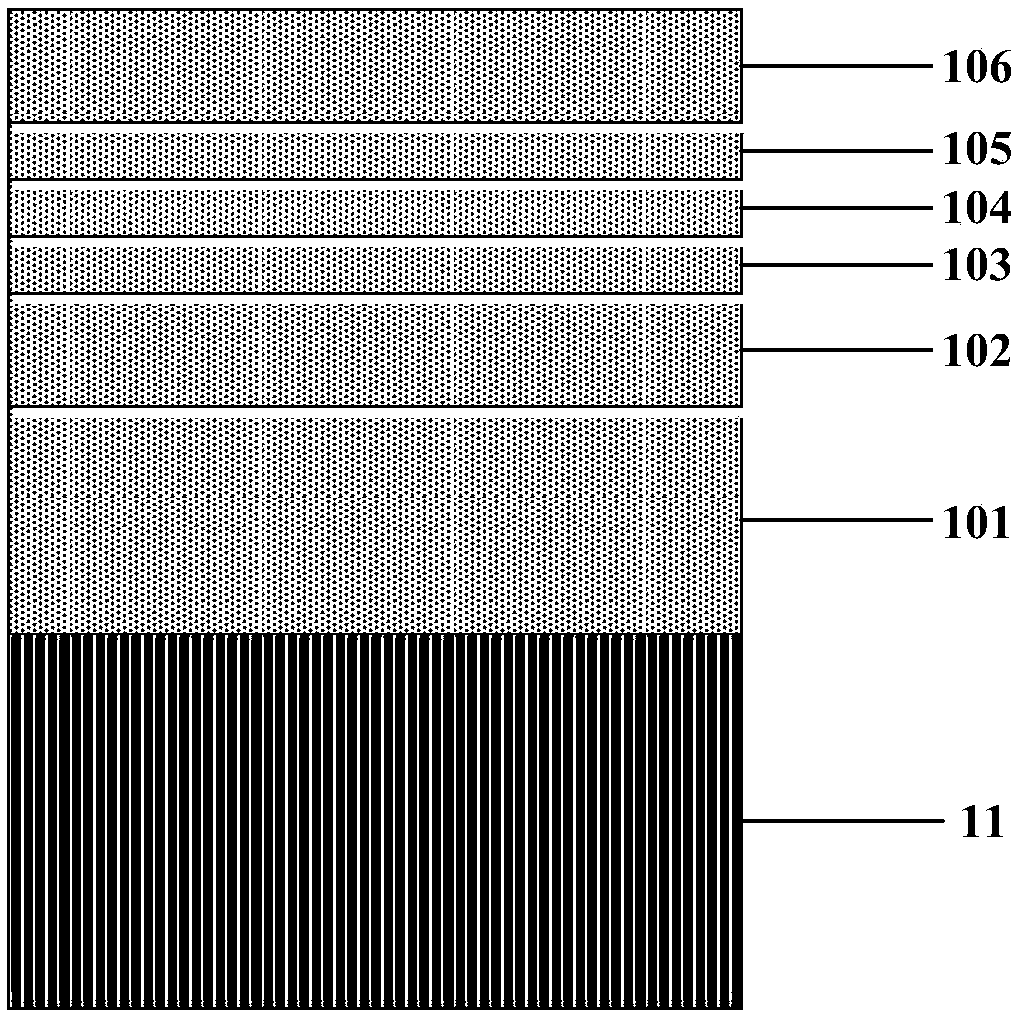
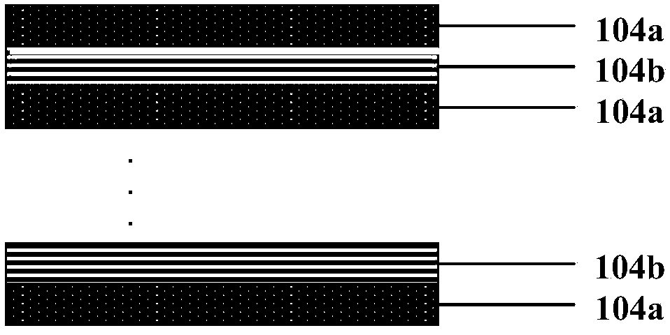
[0094] See Figure 2 to Figure 16 , figure 2 A schematic diagram of the growth of a blue light material provided by an embodiment of the present invention; image 3 A schematic diagram of the growth of a first active layer provided by an embodiment of the present invention; Figure 4 A schematic diagram of the preparation of a yellow light wick groove provided by the embodiment of the present invention; Figure 5 A schematic diagram of the growth of a yellow light material provided by the embodiment of the present invention; Image 6 A schematic diagram of the growth of a second active layer provided by an embodiment of the present invention; Figure 7 A schematic diagram of the preparation of a green light wick groove provided by the embodiment of the present invention; Figure 8 A schematic diagram of the growth of a green light material provided by an embodiment of the present invention; Figure 9 A schematic diagram of the growth of a third active layer provided by a...


PUM

PropertyMeasurementUnit
Thicknessaaaaaaaaaa
Thicknessaaaaaaaaaa
Thicknessaaaaaaaaaa

Abstract

The invention relates to a fabrication method of a novel GaN-based LED. The fabrication method comprises the steps of selecting a sapphire substrate; forming a first blue-light material, a yellow-light material, a green-light material, a red-light material and a second blue-light material which comprises GaN on the sapphire substrate; forming a conductive substrate on surfaces of the first blue-light material, the yellow-light material, the green-light material, the red-light material and the second blue-light material; removing the sapphire substrate; performing surface roughing on back surfaces of the first blue-light material, the yellow-light material, the green-light material, the red-light material and the second blue-light material; and respectively fabricating a positive electrodeand a negative electrode so as to complete fabrication of the novel GaN-based LED. A material with various colors is fabricated in the same LED device, light having various colors is generated, and the defects of low light-emitting efficiency and low integration of the LED device caused by coating fluorescent powder on an LED package device in the prior art can be overcome.

Description

technical field [0001] The invention relates to the technical field of integrated circuits, in particular to a novel GaN-based LED preparation method. Background technique [0002] LED (Lighting Emitting Diode) is a light-emitting diode, which is a semiconductor solid-state light-emitting device. It uses a solid semiconductor chip as a light-emitting material. In the semiconductor, the excess energy is released through the recombination of carriers to cause photon emission, which directly emits red, yellow, blue, and green light. LED is a new type of solid-state light source, which has many advantages such as small size, high luminous efficiency, low energy consumption, long life, no mercury pollution, all solid state, fast response, low working voltage, safety and reliability. [0003] Utilizing the principle of three primary colors, phosphor powder can be added in the packaging of LED devices to emit light of any color, so LEDs can be used as light sources for lighting. ...

Claims


Application Information

Patent Timeline
IPC IPC(8): H01L33/06H01L33/32H01L33/00H01L33/46
CPCH01L33/06H01L33/0075H01L33/32H01L33/46
Inventor 张捷
Owner XIAN ZHISHENG RUIXIN SEMICON TECH CO LTD
Why Eureka
Try Eureka