Vertical transistor and manufacturing method thereof

a technology of vertical transistor and manufacturing method, which is applied in the field of vertical transistor, can solve the problems of difficult to achieve traditional planar transistor performance and difficult to integrate semiconductors, and achieve the effects of reducing the lateral area of transistors, improving device integration and performan

Inactive Publication Date: 2011-05-05
INOTERA MEMORIES INC
View PDF16 Cites 0 Cited by
  • Summary
  • Abstract
  • Description
  • Claims
  • Application Information

AI Technical Summary

Benefits of technology

[0007]The objective of the present invention is to provide a vertical transistor characterized by: reduced lateral area of the transistor, improved device integration and performance, and provision of a manufacturing method of the vertical transistor.

Problems solved by technology

In light of this, integration of the semiconductor is difficult to increase.
The performance of the traditional planar transistor is hard to achieve while it is used on sub-50 nm DRAM technology.

Method used


Image

  • Vertical transistor and manufacturing method thereof
  • Vertical transistor and manufacturing method thereof
  • Vertical transistor and manufacturing method thereof

Examples


Embodiment Construction

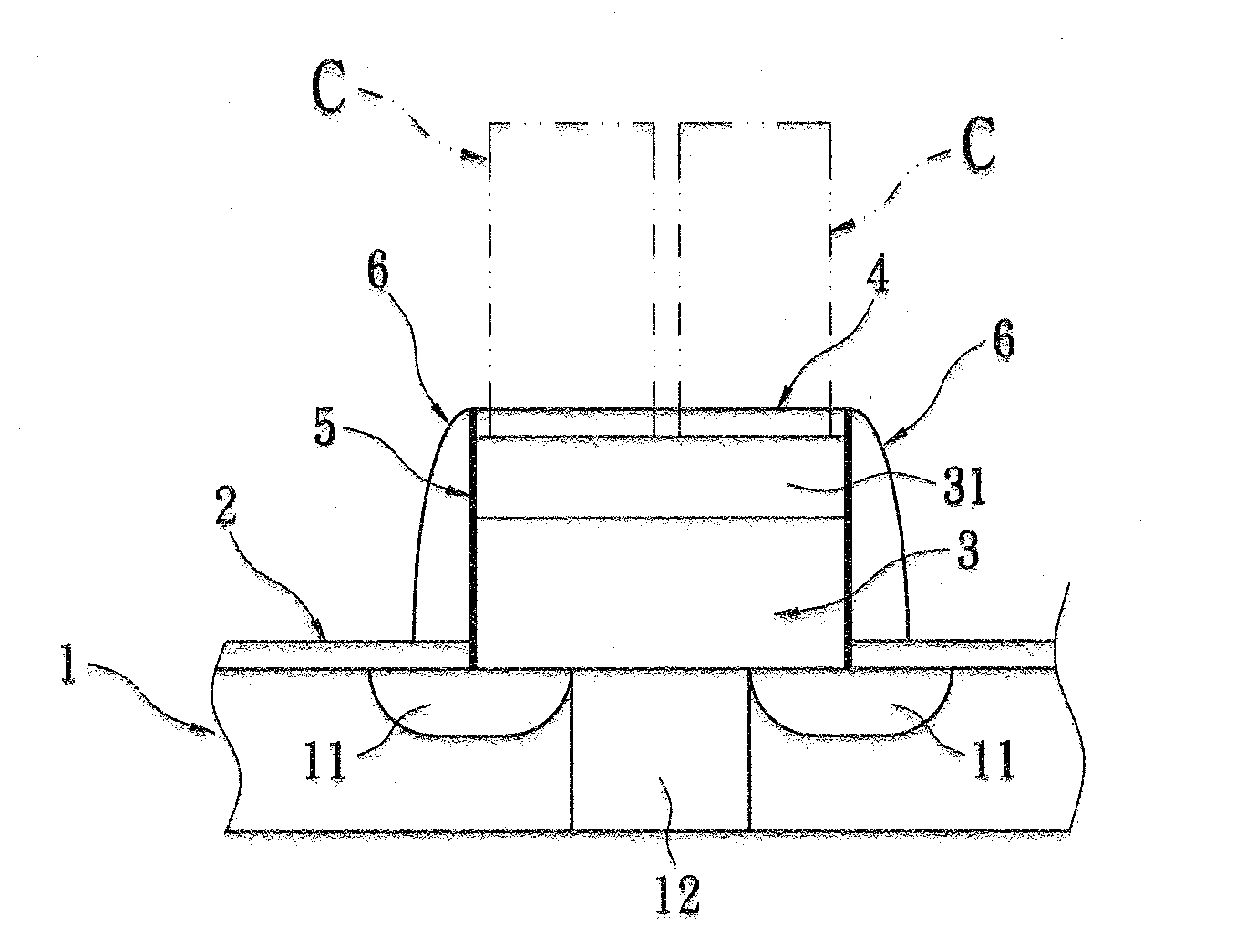
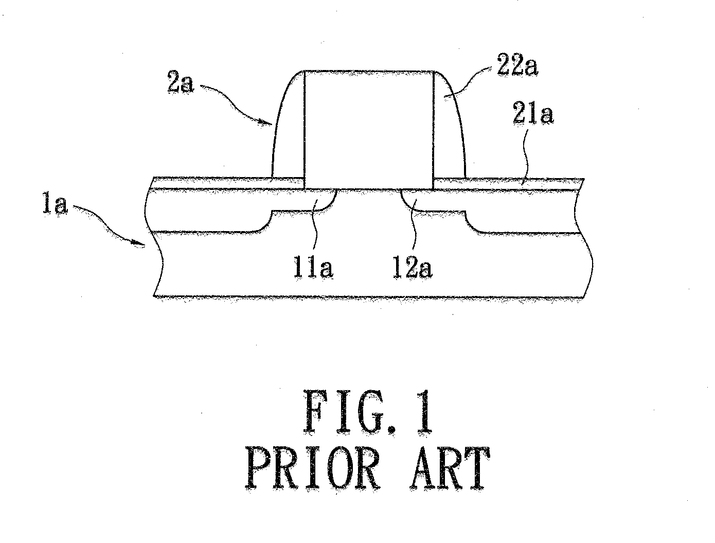
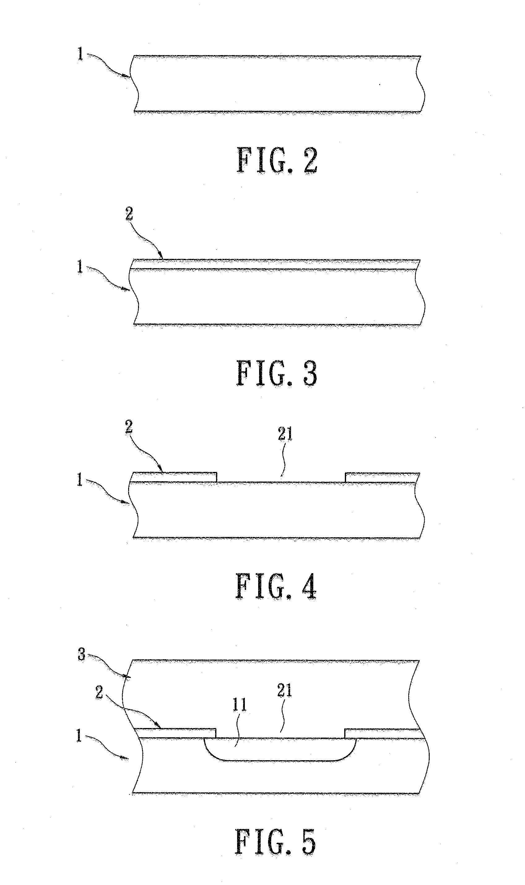
[0028]Refer now to FIGS. 2 to 10, which show the steps of the manufacturing method of a vertical transistor. The vertical transistor manufactured by the method of the present invention can be applied to dynamic random access memory (DRAM). Please refer to FIG. 2; the step (1) is providing a substrate 1, for example, the substrate 1 may be a semiconductor wafer of silicon material.

[0029]Please refer to FIG. 3; the step (2) is forming a bottom-oxide layer 2 on the substrate 1. In the embodiment, the bottom-oxide layer 2 is a silicon oxide which may be formed by a thermal oxidation method.

[0030]Please refer to FIG. 4; the step (3) is defining the pattern of the gate recess 21 on the bottom-oxide layer 2 via lithography process and then etching the defined pattern to form a gate recess 21. In other words, the gate recess 21 is concavely formed in the bottom-oxide layer 2.

[0031]Please refer to FIG. 5; steps (4) and (5) are shown as follows: The donor ions are implanted in the upper part ...


PUM


Abstract

A vertical transistor includes: a substrate, a bottom-oxide layer, an epitaxial silicon layer, an insulating oxide layer, two gate-oxide films and a gate-stacked layer. The bottom-oxide layer is disposed on the substrate, and the bottom-oxide layer has a gate recess concavely formed thereof. The substrate has a first doped area in an upper part corresponding to the gate recess. The epitaxial silicon layer is formed on the gate recess, and the epitaxial silicon layer has a second doped area in an upper part. The insulating oxide layer is disposed on the epitaxial silicon layer. The gate-oxide films are respectively formed on two opposite sides of the epitaxial silicon layer. The gate-stacked layer is formed on the two gate-oxide layers and the bottom-oxide layer. Whereby, the lateral area of transistor is reduced, and the integration and the performance of the device are improved.

Description

BACKGROUND OF THE INVENTION[0001]1. Field of the Invention[0002]The present invention relates to a transistor and its manufacturing method; especially, the present invention relates to a vertical transistor and its manufacturing method.[0003]2. Description of Related Art[0004]As electronics technology develops and improves, manufacturing processes continue placing pressure upon, and necessarily driving, electronic products to evolve toward the smaller size and lighter weight as well as further driving DRAM (dynamic random access memory) designs toward high integration and high density. Please refer to FIG. 1; a traditional planar transistor of DRAM includes a substrate 1a and a gate 2a. The gate 2a is formed on the substrate 1a. Furthermore, a source 11a and a drain 12a are respectively formed in the substrate 1a on two sides of the gate 2a. The gate 2a has an oxide 21a and two spacers 22a. [0005]However, due to the planar arrangement of the source 11a, the drain 12a and the gate 2a...

Claims


Application Information

Patent Timeline
Patent Type & Authority Applications(United States)
IPC IPC(8): H01L29/78H01L21/336
CPCH01L29/42376H01L29/4238H01L29/0847H01L27/10876H01L29/0653H01L29/7827H01L29/66666H10B12/053
Inventor CHEN, HSIN-HUEILEE, CHUNG-YUAN
Owner INOTERA MEMORIES INC
Why Eureka
Try Eureka