Method for improving high-low voltage ESD protection performance by employing well segmentation technology

An ESD protection, low-voltage technology, applied in low-voltage ESD protection design, using well segmentation technology to improve the performance of low-voltage ESD protection devices, can solve the problems of easy latch-up, high trigger voltage, etc., achieve the effect of reducing parasitic capacitance and meeting ESD protection requirements

Active Publication Date: 2018-06-01
JIANGNAN UNIV
View PDF4 Cites 6 Cited by
  • Summary
  • Abstract
  • Description
  • Claims
  • Application Information

AI Technical Summary

Problems solved by technology

[0004] Aiming at problems such as too large chip area occupied by diodes or too high SCR trigger voltage and easy latch-up in ESD protection applications, the present invention provides a method for improving the performance of low-voltage ESD protection devices by using well segmentation technology, which includes well segmentation technology and special The unique metal wiring method can not only select the appropriate number of diodes in series and adjust the trigger voltage of the ESD protection device without increasing the chip area; it can also use the metal wiring method to change the ESD current discharge path inside the device, Adjust the maintenance voltage of the device, enhance the ESD robustness of the device, and can be applied to the design of low-voltage ESD protection devices for RF ICs or different ESD design windows

Method used


Image

  • Method for improving high-low voltage ESD protection performance by employing well segmentation technology
  • Method for improving high-low voltage ESD protection performance by employing well segmentation technology
  • Method for improving high-low voltage ESD protection performance by employing well segmentation technology

Examples


Embodiment Construction

[0024] Below in conjunction with accompanying drawing and specific embodiment the present invention is described in further detail;

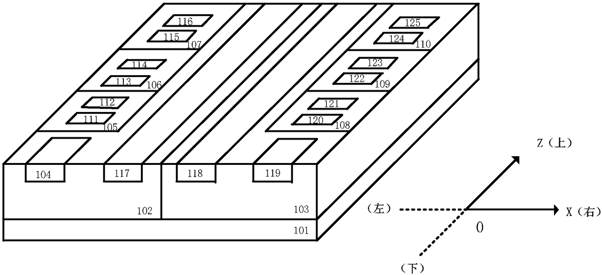
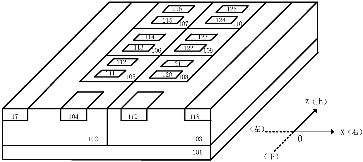
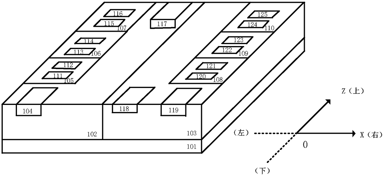
[0025] The example of the present invention has designed a kind of method that utilizes well segmentation technology to improve low-voltage ESD protection performance, and it comprises the ESD current discharge path of SCR and the ESD electric discharge path of diode forward conduction, utilizes well segmentation technology on the one hand, can not only aim at Different protected circuits are designed with different voltages to trigger and turn on the low-voltage ESD protection device. On the other hand, a special metal wiring method is used to adjust the P+ injection region in the first N well and the first P well inside the device. The position of the stripe layout of the N+ injection region changes the sustaining voltage of the low-voltage ESD protection device.

[0026] Such as figure 1 The structure sectional view of the shown method examp...


PUM


Abstract

A method for improving high-low voltage ESD protection performance by employing a well segmentation technology concretely comprises a well segmentation technology and a special metal wiring method toimprove the reliability of on-chip IC low-voltage ESD protection. A device 1 in one embodiment of the invention is mainly formed by a P substrate, a first N well, a first P well, a second P well, a second N well, a third P well, a third N well, a fourth P well, a fourth N well, a fourth P+ injection region and a fifth N+ injection region. Under an ESD stress effect, the well segmentation technology is employed so as to obtain a low-voltage ESD protection device of an SCR triggered by a diode, avoid generation of an avalanche breakdown effect at the internal portion of the device and reduce a triggering voltage of the device and so as to greatly reduce stray capacitance of the device and meet ESD protection demands of a radio frequency IC. Besides, the positions of the N+ injection region and the P+ injection region at the internal portion of the device are regulated to change the ESD current discharge path of the SCR structure, and the method provided by the invention combines the metal wiring design to regulate a maintenance voltage of the device.

Description

technical field [0001] The invention belongs to the field of electrostatic discharge protection of integrated circuits, relates to a low-voltage ESD protection design method, in particular to a method for improving the performance of a low-voltage ESD protection device by using well segmentation technology, which can be used to improve the reliability of on-chip IC low-voltage ESD protection. Background technique [0002] Electrostatic discharge (ESD) is a common phenomenon in nature. Electronic products, especially integrated circuits (ICs), are inevitably damaged by ESD during production, packaging, testing, storage, and transportation. According to the statistics of NationalSemiconductor Corporation of the United States, the failure of IC caused by ESD has become one of the main reasons for the failure of electronic products. With the maturity of RF IC technology, the feature size of semiconductor manufacturing process is getting smaller and smaller, and the application o...

Claims


Application Information

Patent Timeline
Patent Type & Authority Applications(China)
IPC IPC(8): H01L27/02
CPCH01L27/0255H01L27/0296
Inventor 梁海莲刘湖云顾晓峰
Owner JIANGNAN UNIV
Why Eureka
Try Eureka