Flip Chip Butt Bonding Method of Focal Plane Array Detector

A focal plane detector and focal plane array technology, which is applied in the manufacture of semiconductor devices, electric solid-state devices, and semiconductor/solid-state devices, etc. Strong operability and the effect of increasing the contact area

Active Publication Date: 2019-11-05
THE 44TH INST OF CHINA ELECTRONICS TECH GROUP CORP
View PDF3 Cites 0 Cited by
  • Summary
  • Abstract
  • Description
  • Claims
  • Application Information

AI Technical Summary

Problems solved by technology

[0006] The invention provides a focal plane array detector flip-chip welding butt joint method to solve the problem of low alignment accuracy of flip-chip welding at present

Method used


Image

  • Flip Chip Butt Bonding Method of Focal Plane Array Detector
  • Flip Chip Butt Bonding Method of Focal Plane Array Detector
  • Flip Chip Butt Bonding Method of Focal Plane Array Detector

Examples


Embodiment Construction

[0035] In order to enable those skilled in the art to better understand the technical solutions in the embodiments of the present invention, and to make the above-mentioned purposes, features and advantages of the embodiments of the present invention more obvious and understandable, the following describes the technical solutions in the embodiments of the present invention in conjunction with the accompanying drawings For further detailed explanation.

[0036] In the description of the present invention, unless otherwise specified and limited, it should be noted that the term "connection" should be understood in a broad sense, for example, it can be a mechanical connection or an electrical connection, or it can be the internal communication of two elements, it can be Directly connected or indirectly connected through an intermediary, those skilled in the art can understand the specific meanings of the above terms according to specific situations.

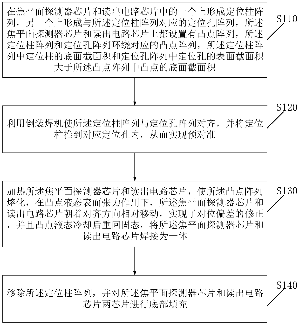
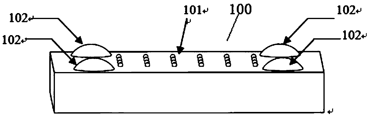
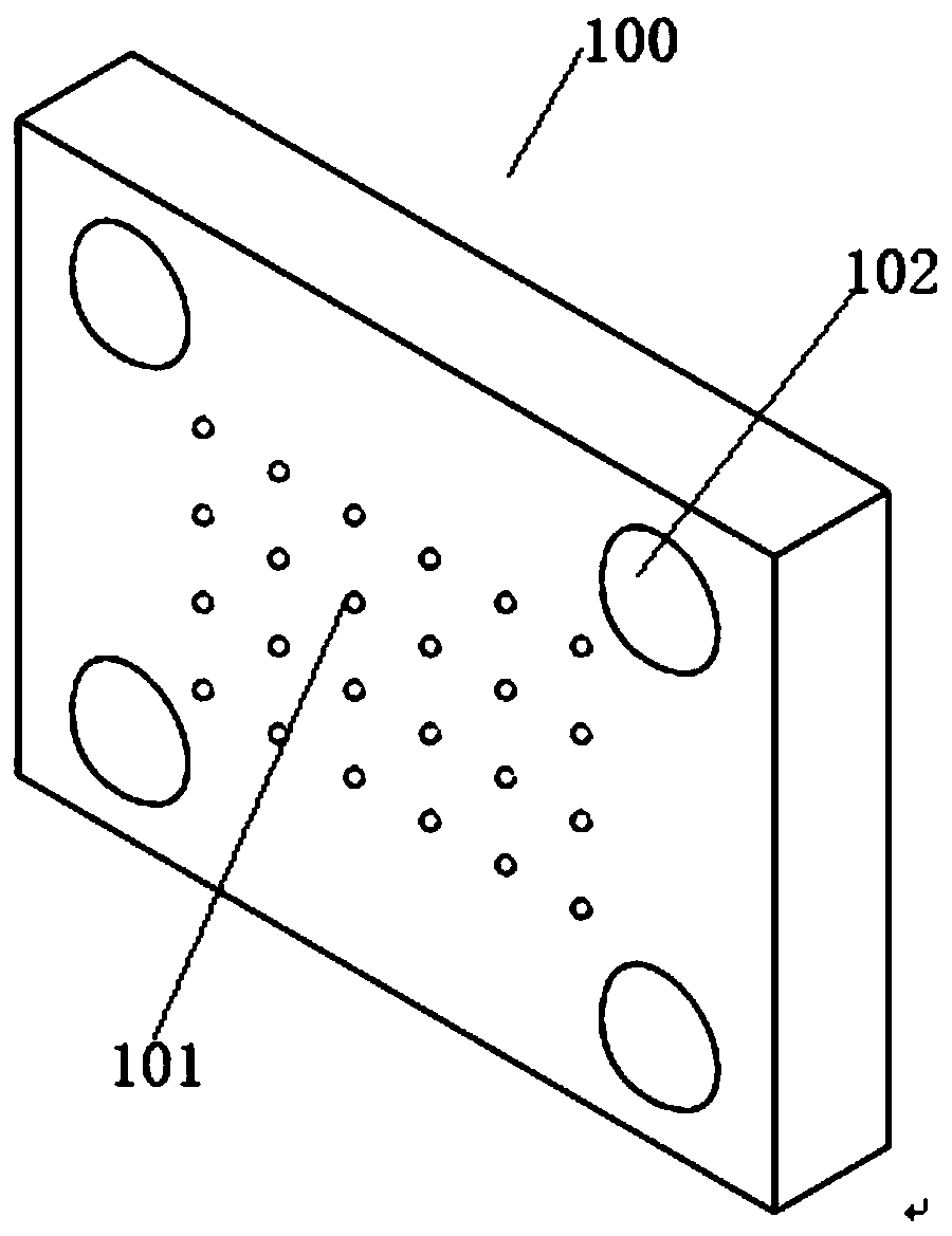
[0037] see figure 1 , is a ...


PUM


Abstract

The invention provides a focal plane array detector flip-chip bonding butt-joint method, which comprises the steps of forming a positioning column array on one of a focal plane detector chip and a readout circuit chip, forming positioning hole array corresponding to the positioning column array on the other chip, wherein both chips are provided with a convex point array, the positioning column array and the positioning hole array surround the corresponding convex point arrays, and the bottom surface sectional area of each positioning column in the positioning column array and the surface sectional area of each positioning hole in the positioning hole array are greater than the bottom surface sectional area of each convex point in the convex point array; enabling the positioning column array to be aligned to the positioning hole array by using a flip-chip bonding machine, and pushing the positioning columns into the corresponding positioning holes so as to achieve pre-alignment; heatingthe two chips, enabling the convex point array to be molten, the two chips move oppositely towards the alignment direction under the liquid surface tension of the convex points so as to realize correction for the alignment deviation, wherein the liquid-state convex points get back to a solid state after being cooled, and the two chips are welded into a whole; and removing the positioning column array. The alignment accuracy is improved according to the invention.

Description

technical field [0001] The invention belongs to the technical field of semiconductors, and in particular relates to a focal plane array detector flip-chip welding butt joint method. Background technique [0002] Flip-chip welding is a high-performance semiconductor chip assembly technology. This technology is based on the distribution of detection units on the focal plane detector chip PDA (Photo-Diode Array, photodiode array), and prepares electrodes on each detection unit. Spherical solder, so that the bump arrays are formed on the focal plane detector chip and the readout circuit chip respectively, and the focal plane detector chip PDA and the corresponding readout circuit chip ROIC (Read out integrated circuit, read out integrated circuit) ) for alignment welding to form a focal plane device FPA (Focal plane array, focal plane array). The bump array between the focal plane detector chip PDA and the readout circuit chip ROIC forms several independent signal transmission ...

Claims


Application Information

Patent Timeline
Patent Type & Authority Patents(China)
IPC IPC(8): H01L21/60H01L31/102
CPCH01L24/10H01L31/102H01L2021/60022
Inventor 董绪丰陈扬柳聪黄晓峰
Owner THE 44TH INST OF CHINA ELECTRONICS TECH GROUP CORP
Why Eureka
Try Eureka