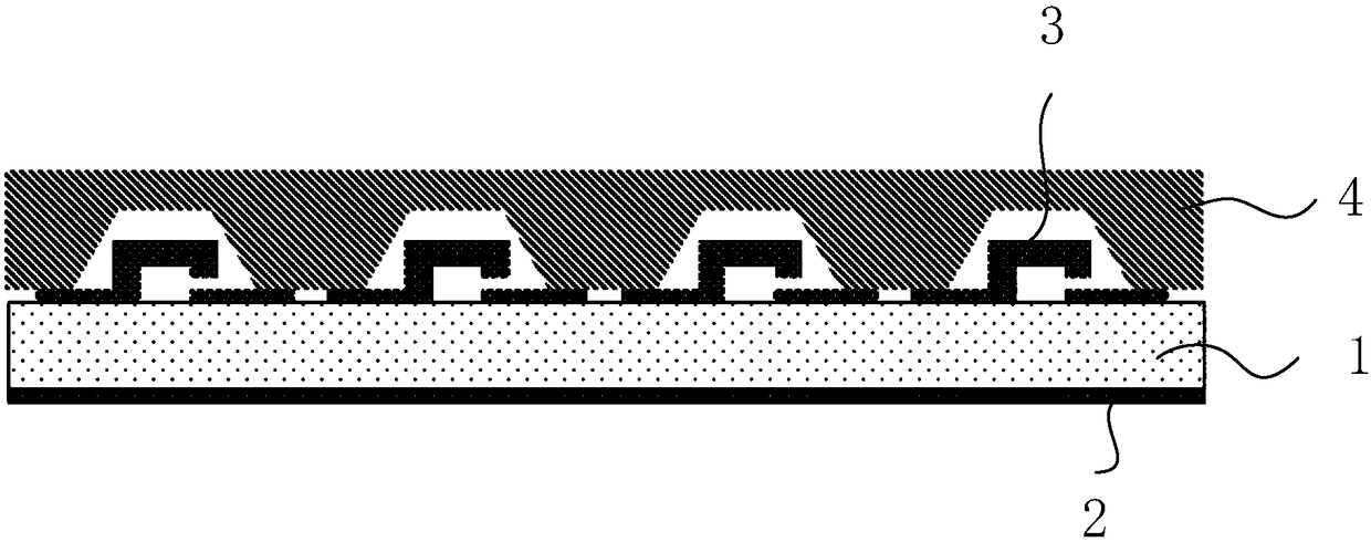
Method for preparing high-performance radio frequency micro-electro-mechanical system (MEMS) switch and MEMS switch
A technology of micro-electromechanical switch and micro-electro-mechanical system, which is applied in the components of TV system, generator/motor, micro-electronic micro-structure device, etc., can solve the problems of difficulty in automatic operation, bottleneck in performance improvement, and improve work efficiency. , to ensure reliability and reduce costs
- Summary
- Abstract
- Description
- Claims
- Application Information
AI Technical Summary
Problems solved by technology
Method used
Image
Examples
Embodiment 1
[0038] According to the embodiment, a glass substrate is first used, and then a layer of 100nm-500nm doped amorphous silicon film is deposited on the bottom surface of the substrate using a low-temperature process, and then a surface micromachining process and a conventional MEMS process The electromechanical switch is fabricated on the top surface of the substrate; then the adhesive bonding method is used to complete the high air-tight cap processing of the microelectromechanical switch, and finally, the single-sided dry peeling process is used to remove the opaque film from The bottom surface of the substrate is peeled off, and the cap and the substrate are diced through the invisible dicing process, so that each MEMS switch is an independent switch.
Embodiment 2
[0040] According to the embodiment, a glass substrate is first used, and then a layer of 500nm-800nm metal aluminum film is sputtered on the bottom surface of the substrate, and then a surface micromachining process and a conventional MEMS process are used to fabricate the microelectromechanical switch On the top surface of the substrate; then use the anodic bonding method to complete the high air-tight cap processing of the microelectromechanical switch, and finally, use the double-sided wet peeling process to remove the opaque material film from the bottom surface of the substrate Stripping, and dicing the cap and the substrate through the invisible dicing process, so that each MEMS switch is an independent switch.
Embodiment 3
[0042] According to the embodiment, a glass substrate is first used, and then a 500nm metal aluminum film is sputtered on the bottom surface of the substrate. Then, the surface micromachining process and the conventional MEMS process are used to fabricate the metal contact switch on the substrate. The top surface of the substrate; then the anodic bonding method is used to complete the high air-tightness capping treatment of the metal contact switch, and finally, the single-sided wet peeling process is used to remove the opaque material film from the bottom surface of the substrate Stripping, and dicing the cap and the substrate by dicing with a grinding wheel, so that each MEMS switch is an independent switch.
[0043] The present invention has at least the following advantages:
[0044] 1. The present invention uses low-cost glass as a substrate, which effectively reduces its cost.
[0045] 2. The present invention uses glass as the substrate to ensure the high performance of the M...
PUM
 Abstract
Description
Claims
Application Information


