Supercharge Your Innovation With Domain-Expert AI Agents!

Buried metal block pcb and manufacturing method thereof

A manufacturing method and technology of burying metal, which are applied in multilayer circuit manufacturing, printed circuit manufacturing, circuit thermal devices, etc., can solve the problem of not being able to meet the requirements of chip heat dissipation and ultra-high flatness at the same time, and avoid uneven thickness of the board. , good heat dissipation performance, improve the effect of flatness

Active Publication Date: 2020-04-10
GUANGZHOU FASTPRINT CIRCUIT TECH +2
View PDF6 Cites 0 Cited by
  • Summary
  • Abstract
  • Description
  • Claims
  • Application Information

AI Technical Summary

Problems solved by technology

However, limited by the industry's technological capabilities, the height difference between the metal block and the PCB surface is about 3 mils (1 mil = 25.4 microns). The flatness requirement of the block area is that the height drop is less than 10 microns, which far exceeds the existing industry production capacity
Therefore, the current technology cannot meet the requirements of chip heat dissipation and ultra-high flatness at the same time

Method used


Image

  • Buried metal block pcb and manufacturing method thereof
  • Buried metal block pcb and manufacturing method thereof
  • Buried metal block pcb and manufacturing method thereof

Examples


Embodiment Construction

[0037] In order to make the object, technical solution and advantages of the present invention clearer, the present invention will be further described in detail below in conjunction with the accompanying drawings and specific implementation methods. It should be understood that the specific embodiments described here are only used to explain the present invention, and do not limit the protection scope of the present invention.

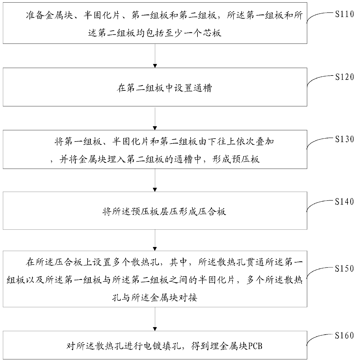
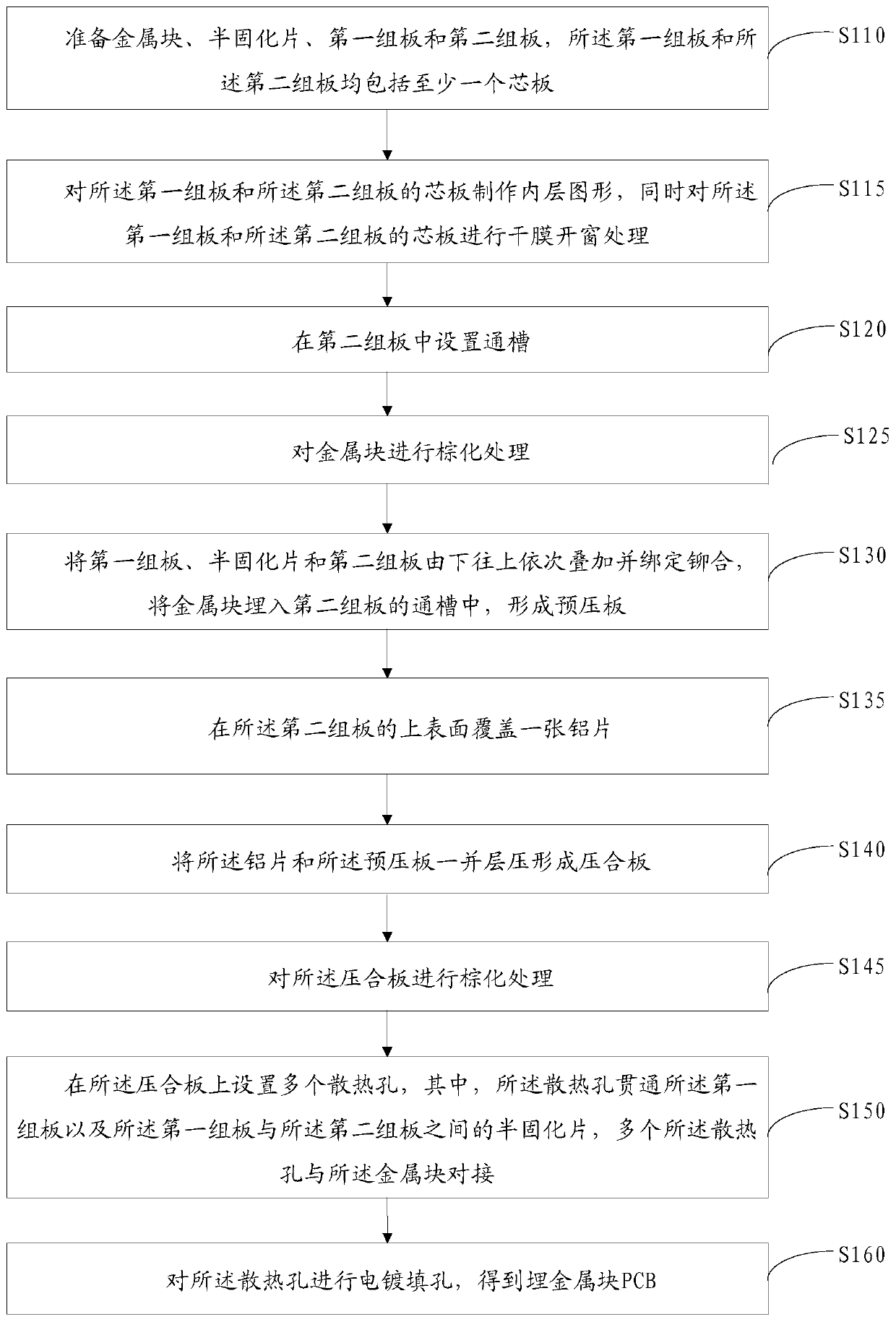
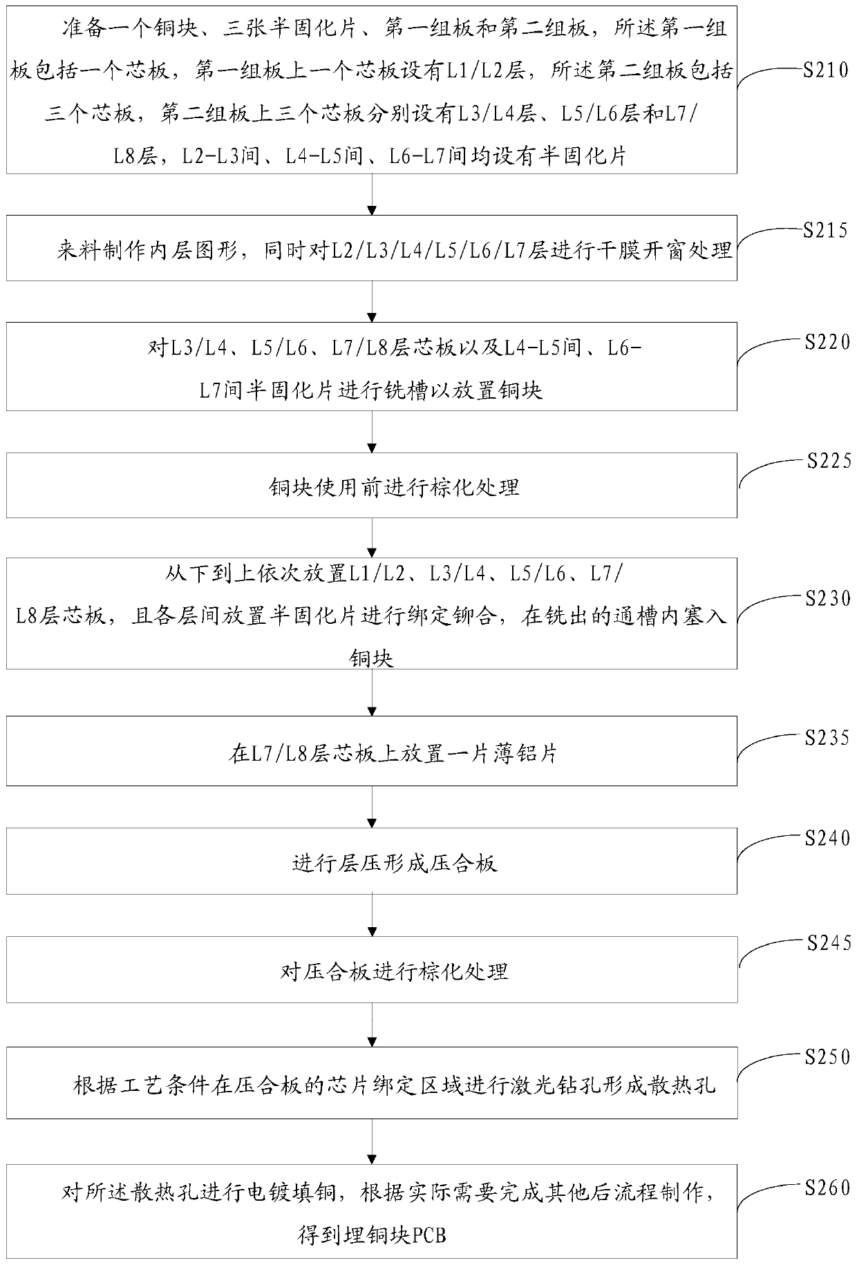
[0038] see figure 1 , Figure 4 and Figure 5 , an embodiment of a method of manufacturing a buried metal block PCB in an embodiment of the present invention, comprising the following steps:

[0039] S110 : Prepare a metal block 300 , a prepreg 200 , a first group of boards 10 and a second group of boards 20 , each of the first group of boards 10 and the second group of boards 20 includes at least one core board 100 .

[0040] When there are two or more core boards 100 in the first group of boards 10 and the second group of boards 20, the core boar...


PUM


Abstract

The invention discloses a metal block-embedded PCB and a manufacturing method thereof. The manufacturing method of the metal block-embedded PCB comprises the following steps of preparing a metal block, a prepreg, a first group plate and a second group plate, wherein each of the first group plate and the second group plate comprises at least one core plate; setting a through groove in the second group plate; enabling the first group plate, the prepreg and the second group plate to be stacked from the bottom up, and enabling the metal block to be embedded in the through groove of the second group plate to form a pre-pressing plate; putting the pre-pressing plate into a lamination apparatus to be laminated to form a pressing plate; setting multiple heat dissipation holes in the pressing plate, wherein the heat dissipation holes run through the first group plate and the prepreg between the first group plate and the second group plate, and the multiple heat dissipation holes are in butt joint with the metal block; and performing electroplating hole filling on the heat dissipation holes to obtain the metal block-embedded PCB. By virtue of the manufacturing method, high smoothness of thesurface of the PCB can be ensured, the bonding performance of the chip can be ensured, and excellent heat dissipation performance can be achieved.

Description

technical field [0001] The invention relates to the technical field of printed circuit boards, in particular to a buried metal block PCB and a manufacturing method thereof. Background technique [0002] With the continuous improvement of chip manufacturing process, hundreds of millions or even billions of transistors are placed in smaller and smaller chips. Big. The stability of chip operating temperature is crucial to chip performance. The packaging mode of the chip affects the heat dissipation efficiency of the chip to a certain extent. Among the many packaging methods, COB (chip on board) packaging has become the preferred packaging mode to solve the problem of chip heat dissipation because of its efficient thermal management mode. , and it also has the advantages of saving space and simple manufacturing process. The COB package is to directly stick the bare chip on the PCB (Printed Circuit Board, printed circuit board) through thermal conductive adhesive, and connect ...

Claims


Application Information

Patent Timeline
Patent Type & Authority Patents(China)
IPC IPC(8): H05K1/02H05K3/46
CPCH05K1/0204H05K3/4611H05K2201/09563H05K2201/10416
Inventor 李星史宏宇李志东
Owner GUANGZHOU FASTPRINT CIRCUIT TECH
Features
  • R&D
  • Intellectual Property
  • Life Sciences
  • Materials
  • Tech Scout
  • Unparalleled Data Quality
  • Higher Quality Content
  • 60% Fewer Hallucinations
Learn More