Grid voltage bootstrap switch circuit

A switch circuit and grid voltage bootstrap technology, which is applied in the field of grid voltage bootstrap switch circuits, can solve the problems of reduced circuit life, circuit reliability, and large size, and achieves improved linearity, improved reliability, and reduced conduction The effect of resistance

Active Publication Date: 2018-06-12
UNIV OF ELECTRONICS SCI & TECH OF CHINA
View PDF5 Cites 10 Cited by
  • Summary
  • Abstract
  • Description
  • Claims
  • Application Information

AI Technical Summary

Problems solved by technology

[0011] However, in a traditional gate voltage bootstrap circuit, M 2 The overvoltage state in the turn-off phase will cause reliability problems of the circuit and reduce the life of the circuit; generally, in order to realize fast sampling of high-speed signals, th

Method used


Image

  • Grid voltage bootstrap switch circuit
  • Grid voltage bootstrap switch circuit
  • Grid voltage bootstrap switch circuit

Examples


Embodiment Construction

[0042] The technical solution of the present invention will be described in detail below in conjunction with the accompanying drawings and specific embodiments.

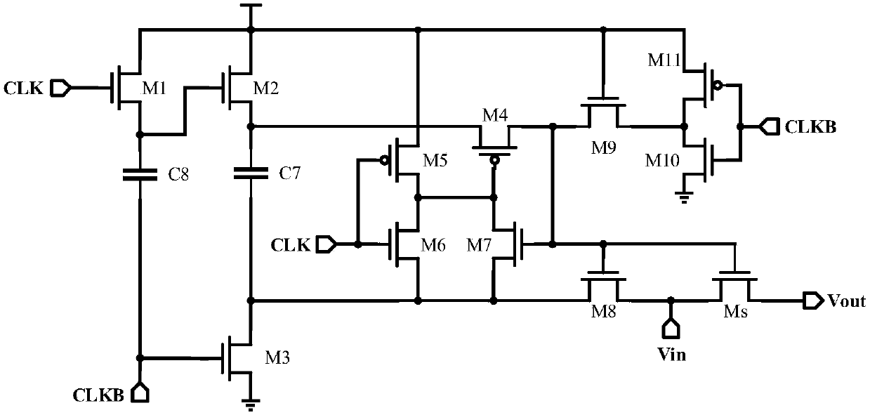
[0043] Such as figure 2 As shown, a gate voltage bootstrap switch circuit provided by the present invention includes an NMOS main switch tube M n and PMOS main switch M p , and with the NMOS main switch M n The connected first charge pump circuit, grid voltage boosting circuit and first switch circuit, and the PMOS main switch tube M p The connected second charge pump circuit, gate voltage drop circuit and second switch circuit, NMOS main switch tube M n The source is connected to the PMOS main switch M p The source is connected to the input signal V as the input terminal of the gate voltage bootstrap switch circuit in , whose drain is connected to the PMOS main switch M p The drain is connected as the output of the gate voltage bootstrap switch circuit to the output signal V out , the input signal V in Conn...


PUM


Abstract

The invention provides a grid voltage bootstrap switch circuit, and belongs to the field of analog integrated circuits. A charge pump circuit is used for charging a fifth capacitor and a sixth capacitor to make the stored charge amounts be constant, a grid voltage boosting circuit and a grid voltage reducing circuit are used for changing the grid voltages of an NMOS switch tube and a PMOS switch tube to maintain the grid voltages as constant values, and a switching circuit is used for controlling the charging of the charge pump circuit and the opening and closing of the grid voltage boosting circuit and the grid voltage reducing circuit. The grid voltage bootstrap switch circuit provided by the invention uses the NMOS switch tube and the PMOS switch tube to connect input signals to the output at the same time, thereby reducing the on-resistance of the switch; by using a parallel connection mode of the NMOS switch tube and the PMOS switch tube, the channel charge injection effects of the NMOS switch tube and the PMOS switch tube caused by clock changes cancel each other, and the clock feedthrough effects cancel each other as well, thereby improving the linearity of the switch; and by using a diode to charge the capacitor, the circuit does not have an overvoltage device, thus improving the reliability of the circuit.

Description

technical field [0001] The invention belongs to the field of analog integrated circuit design, in particular to a gate voltage bootstrap switch circuit. Background technique [0002] With the continuous development of modern communication technology and the continuous improvement of people's requirements for communication speed, the frequency of analog signals in communication systems continues to increase, and the requirements for converting analog signals into digital signals continue to increase. Higher linearity when sampling an analog signal requires the use of a gate voltage bootstrap circuit. [0003] The traditional gate voltage bootstrap switch circuit structure such as figure 1 As shown, by the main switch tube M s and a gate voltage bootstrap circuit, where the gate voltage bootstrap circuit includes a capacitor C 7 ~C 8 and MOS transistor M 1 ~ M 11 . Its working principle is: [0004] (1) Off phase: when CLK is low and CLKB is high, M 3 conduction, C 7...

Claims


Application Information

Patent Timeline
IPC IPC(8): H03K17/687
CPCH03K17/687
Inventor 李靖魏祎宁宁
Owner UNIV OF ELECTRONICS SCI & TECH OF CHINA
Why Eureka
Try Eureka