Photoelectric detector

A photodetector and photodetection technology, which is applied in the field of photodetectors, can solve problems such as inability to resist radiation, and achieve the effects of reduced irradiation dose, stable structure, and small damage

Active Publication Date: 2018-06-15
GUIZHOU MINZU UNIV
View PDF4 Cites 9 Cited by
  • Summary
  • Abstract
  • Description
  • Claims
  • Application Information

AI Technical Summary

Problems solved by technology

[0004] In view of the above problems, the present invention provides a photodetector, which effectively solves the technical problem that the existing photodetectors cannot resist radiation

Method used


Image

  • Photoelectric detector
  • Photoelectric detector
  • Photoelectric detector

Examples


Embodiment Construction

[0025] In order to explain the embodiments of the present invention or the technical solutions in the prior art more clearly, the specific embodiments of the present invention will be described below with reference to the drawings. Obviously, the drawings in the following description are only some embodiments of the present invention. For those of ordinary skill in the art, without creative work, other drawings can be obtained based on these drawings and obtained Other embodiments.

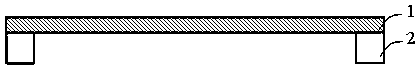
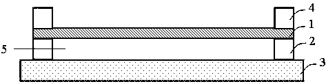
[0026] Such as figure 1 Shown is a schematic structural diagram of an embodiment of the photodetector provided by the present invention. It can be seen from the figure that the photodetector includes: a photodetection layer 1 and a first electrode layer 2, and the first electrode layer is arranged On one side surface of the photodetection layer, a photodetection structure is obtained; the photodetection layer is made of a two-dimensional material or a two-dimensional material heterostructure.

[0027]...


PUM


Abstract

The invention provides a photoelectric detector. The photoelectric detector comprises a photoelectric detection layer and a first electrode layer, wherein the first electrode layer is arranged on a surface of one side of a photoelectric layer to obtain a photoelectric detection structure, and the photoelectric detection layer is formed by fabrication of a two-dimensional material or a two-dimensional material heterojunction structure. Since the two-dimensional material or the two-dimensional material heterojunction structure is sensitive to light and is simultaneously thin (the thickness is smaller than 1 nanometer), the probability of reaction with radiation particles is extremely small, and the false triggering probability is extremely small; and moreover, an acting force among atoms ina two-dimensional material plane is relatively high, the photoelectric detector is stable in structure, and the damage generated by the radiation particle is relatively small.

Description

Technical field [0001] The present invention relates to the field of semiconductor technology, in particular to a photodetector. Background technique [0002] With the development of aerospace technology, various new types of artificial satellites and spacecraft have been put into space. In order to achieve more functions, artificial satellites and spacecraft carry a large number of electronic and optoelectronic devices. However, spacecraft in space will be exposed to various radiations, which can cause serious damage to integrated electronic chips, affect the performance of devices, and even damage these integrated electronic chips, causing irreparable losses. [0003] In addition, in the nuclear industry, a large number of intelligent chips are also needed. Especially in the rescue of nuclear accidents, precision electronic and optoelectronic devices such as robots are required. Nuclear weapon explosions will also pose a serious threat to various electronic and optoelectronic co...

Claims


Application Information

Patent Timeline
Patent Type & Authority Applications(China)
IPC IPC(8): H01L31/0203H01L31/028H01L31/032H01L31/09H01L31/109H01L31/08H01L31/118H01L25/04H01L23/552B82Y30/00B82Y40/00
CPCB82Y30/00B82Y40/00H01L23/552H01L25/043H01L31/0203H01L31/028H01L31/032H01L31/085H01L31/09H01L31/109H01L31/118
Inventor 刘江涛
Owner GUIZHOU MINZU UNIV
Why Eureka
Try Eureka