

Image processing apparatus and system, electronic device and image processing method
An image processing device and image processing technology, applied in image communication, TV system components, TV, etc., can solve the problems of not being able to guarantee the starting point of exposure time, easy to produce differences in integral energy, and differences in exposure amount, etc., with a simple approach Reliable, performance-enhancing, flicker-free effects
- Summary
- Abstract
- Description
- Claims
- Application Information
AI Technical Summary
Problems solved by technology
Method used
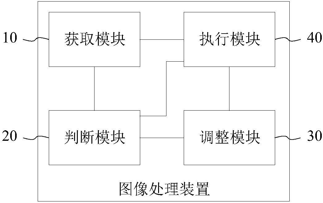
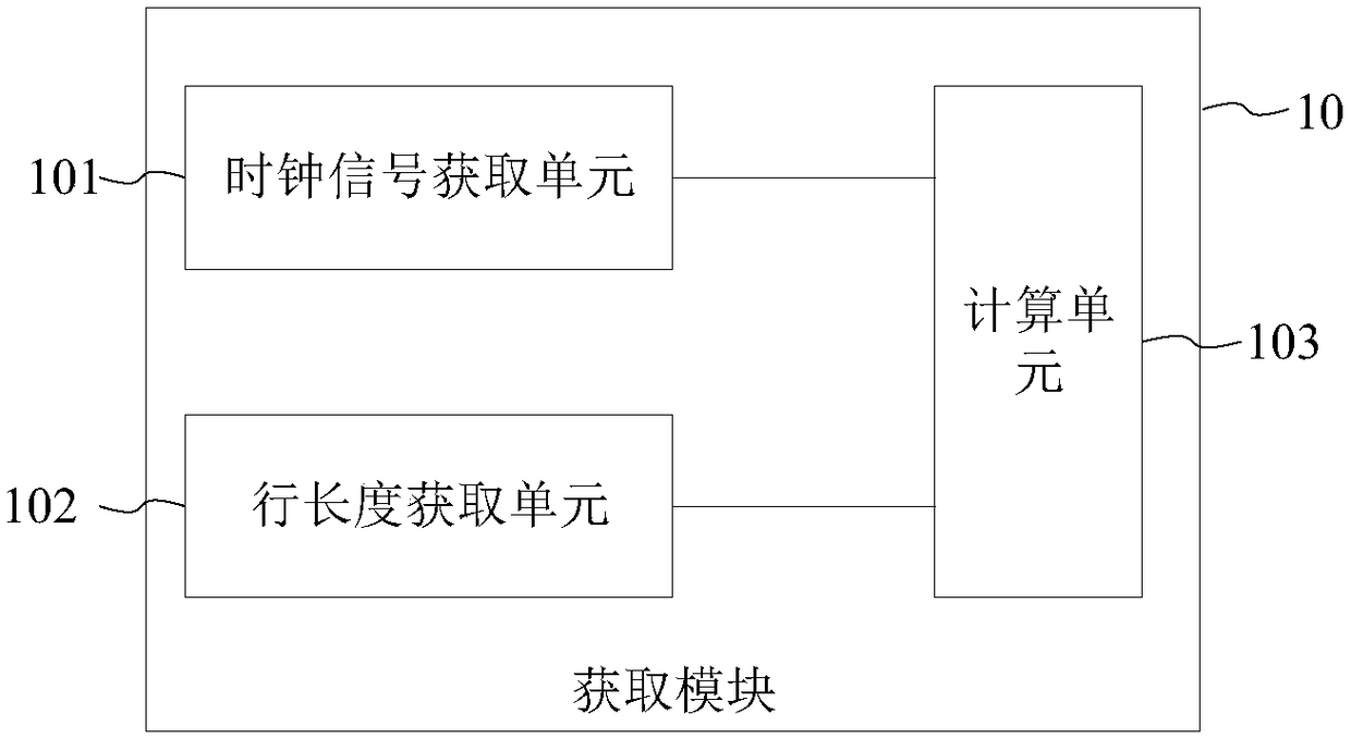
Image

Examples
Embodiment Construction
[0038] In order to make the purpose, technical solutions and advantages of the embodiments of the present invention clearer, the technical solutions in the embodiments of the present invention will be clearly and completely described below in conjunction with the drawings in the embodiments of the present invention. Obviously, the described embodiments It is a part of embodiments of the present invention, but not all embodiments. Based on the embodiments of the present invention, all other embodiments obtained by persons of ordinary skill in the art without making creative efforts belong to the protection scope of the present invention.
[0039] It should be noted that in this document, relational terms such as "first", "second", "third", etc. (if any) are only used to distinguish one entity or operation from another entity or operation, and No such actual relationship or order between these entities or operations is necessarily required or implied. It is to be understood tha...
PUM
 Abstract
Description
Claims
Application Information