On-chip mode multiplexing and demultiplexing device
A mode demultiplexing and mode multiplexing technology, applied in the field of optical communication transmission, can solve problems such as small processing tolerance, reduced device performance, and increased mode loss
- Summary
- Abstract
- Description
- Claims
- Application Information
AI Technical Summary
Problems solved by technology
Method used
Image
Examples
Embodiment Construction
[0042] The present invention will be described in further detail below through specific embodiments and accompanying drawings.
[0043] Below in conjunction with the overall structure of this embodiment figure 1 The implementation of the overall structure is described in detail, figure 1 It includes three parts: mode multiplexing structure, bus waveguide (bus waveguide, a waveguide for transmitting multiple mode signals, which is the carrier of signal transmission in mode division multiplexing system), and mode demultiplexing structure. The bus waveguide can be a waveguide in an integrated device or an optical fiber, depending on the specific application scenario.
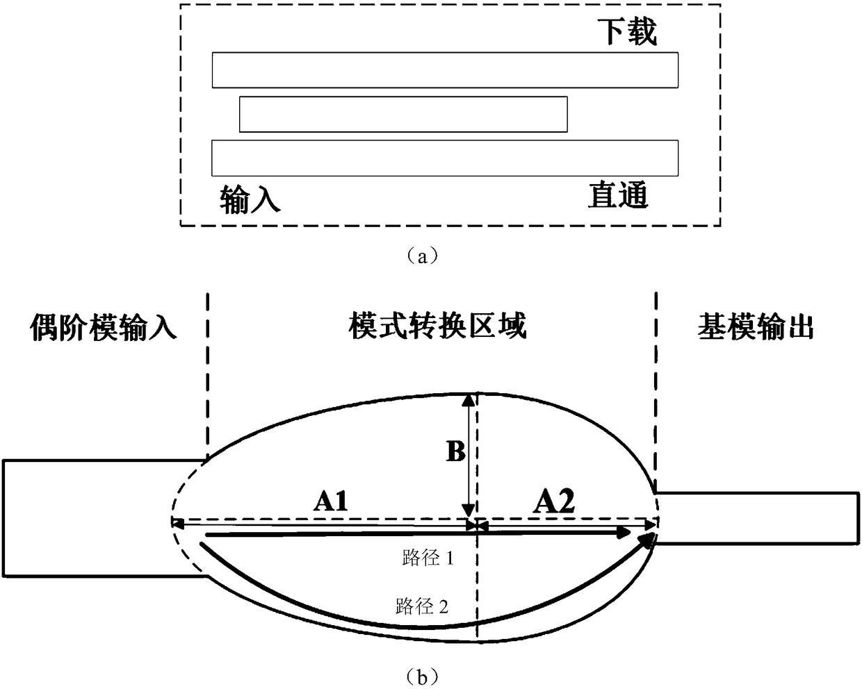
[0044] The pattern multiplexing and demultiplexing structure can be completely symmetrical. The specific details of the mode demultiplexer are given by figure 2 illustrate. The structure consists of four stages, each of which consists of a bridge coupler and a corresponding mode converter (the shape is determi...
PUM
 Abstract
Description
Claims
Application Information


