Thin-film AlGaInP light-emitting diode chip and its preparation method

A light-emitting diode, thin-film technology, applied in electrical components, circuits, semiconductor devices, etc., can solve the problem of light extraction efficiency of less than 10%, and achieve the effect of improving electro-optical conversion efficiency, improving identification, and reducing shading effects.

Pending Publication Date: 2018-06-22
NANCHANG UNIV +1
View PDF12 Cites 14 Cited by
  • Summary
  • Abstract
  • Description
  • Claims
  • Application Information

AI Technical Summary

Problems solved by technology

[0003] In recent years, people have made great progress in epitaxial growth technology. The internal quantum efficiency of AlGaInP light-emitting diodes can reach more than 90%, while conventional structure chips are affected by substrate absorption and total reflection loss, and the light extraction efficiency is less than 10%. , so the electro-optical conversion efficiency is only about 8%

Method used


Image

  • Thin-film AlGaInP light-emitting diode chip and its preparation method
  • Thin-film AlGaInP light-emitting diode chip and its preparation method
  • Thin-film AlGaInP light-emitting diode chip and its preparation method

Examples


Embodiment Construction

[0036] The present invention will be described in detail below in conjunction with the accompanying drawings and embodiments.

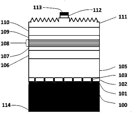
[0037] image 3 As shown, a thin-film AlGaInP light-emitting diode chip includes: a bonding substrate 300 with front and back sides; from the front of the bonding substrate 300 upwards are: substrate side metal bonding layer 301, epitaxial material side metal bonding layer 302, the P-surface diffusion barrier metal layer 303 and the P-surface reflective ohmic contact layer 304, the P-surface reflective ohmic contact layer 304 is an Ag or Ni / Ag laminated structure, and forms a good ohmic contact with the P-type current spreading layer 305, and has Light reflection and ohmic contact function; from the P surface reflection ohmic contact layer 304, there are P-type current spreading layer 305, P-type confinement layer 306, P-side space layer 307, multi-quantum well light-emitting region 308, N-side space layer 309, N-type confinement layer 310 , N-type r...


PUM

PropertyMeasurementUnit
widthaaaaaaaaaa
thicknessaaaaaaaaaa
internal quantum efficiencyaaaaaaaaaa

Abstract

The invention discloses a thin-film AlGaInP light-emitting diode chip and its preparation method. The light-emitting diode chip comprises a bonding substrate with positive and negative faces. From thefront surface of the bonding substrate upwards, it is sequentially provided with: a substrate side metal bonding layer, an epitaxial side metal bonding layer, a P surface diffusion barrier metal layer and a P surface reflection ohm contact layer; from the P surface reflection ohm contact layer to the top, it is sequentially provided with P-type current spreading layer, the P-type limiting layer,the P-side spatial layer, the multi-quantum well light-emitting region, the N-side spatial layer, the N-type limitation layer, the N-type coarse layer, the N-type ohm contact layer and the N electrode; and the reverse side of the bonding substrate is a P electrode. The P-plane reflecting ohm contact layer adopted by the invention has the functions of light reflection and ohm contact; by optimizingthe spacing distance of the block and the width of the N electrode through the blocking of the P-plane reflection ohm contact layer, the current injection concentration problem of the N-electrode corresponding region can be suppressed, and the N electrode shielding effect can be effectively reduced. The invention has the advantages of effectively improving the photoelectric conversion efficiency,simple structure and the like.

Description

technical field [0001] The invention relates to the field of semiconductor light-emitting devices, in particular to a thin-film AlGaInP light-emitting diode chip and a preparation method thereof. Background technique [0002] Semiconductor light-emitting diodes (Light-Emitting Diodes, LEDs) have been widely used in many fields, and are recognized as a next-generation green lighting source. The AlGaInP material lattice-matched with the gallium arsenide substrate can cover visible light wavelengths from 560nm to 650nm, and is an excellent material for preparing red to yellow-green LEDs. AlGaInP-LEDs have important applications in the field of solid-state lighting, such as full-color screen displays, automotive lights, backlights, traffic lights, and daily lighting. [0003] In recent years, people have made great progress in epitaxial growth technology. The internal quantum efficiency of AlGaInP light-emitting diodes can reach more than 90%, while conventional structure chips...

Claims


Application Information

Patent Timeline
Patent Type & Authority Applications(China)
IPC IPC(8): H01L33/40H01L33/38H01L33/00
CPCH01L33/0062H01L33/38H01L33/40H01L33/405
Inventor 李树强陈芳郭醒吴小明王光绪刘军林江风益
Owner NANCHANG UNIV
Why Eureka
Try Eureka