Shift register unit, gate drive circuit, display panel and display device

A shift register and circuit technology, applied in the fields of display panels, display devices, gate drive circuits, and shift register units, can solve the problem of complex gate drive circuit structure design, disadvantageous ultra-narrow frame design, large display panel space, etc. question

Active Publication Date: 2018-06-29
BOE TECH GRP CO LTD +1
View PDF3 Cites 15 Cited by
  • Summary
  • Abstract
  • Description
  • Claims
  • Application Information

AI Technical Summary

Problems solved by technology

Since the gate lines of each row are correspondingly connected to a shift register unit, the structural design of the gate drive circuit is complicated, and the space occupied by the display panel is relatively large, which is not conducive to the ultra-narrow bezel design

Method used


Image

  • Shift register unit, gate drive circuit, display panel and display device
  • Shift register unit, gate drive circuit, display panel and display device
  • Shift register unit, gate drive circuit, display panel and display device

Examples


Embodiment 1

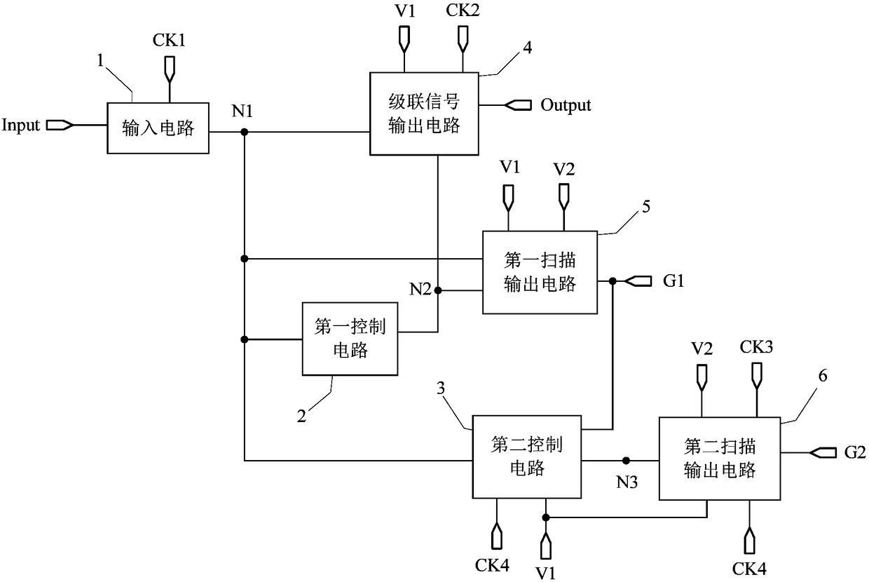
[0111] Such as Figure 3ashown, select Figure 3a There are four stages in the circuit timing diagram shown: the first stage T1, the second stage T2, the third stage T3 and the fourth stage T4.

[0112] In the first stage T1, Input=1, CK1=1, CK2=0, CK3=0, CK4=0.

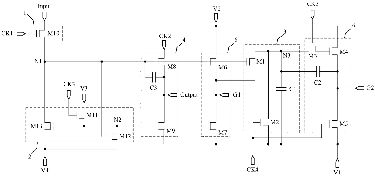
[0113] Since CK1=1, the tenth switching transistor M10 is turned on to provide the high-level signal of the input signal terminal Input to the first node N1, so that the signal of the first node N1 is a high-level signal. Since the signal of the first node N1 is a high level signal, the first switch transistor M1 , the sixth switch transistor M6 , the eighth switch transistor M8 and the twelfth switch transistor M12 are all turned on. The turned-on twelfth switch transistor M12 provides the low-level signal of the fourth reference signal terminal V4 to the second node N2, making the signal of the second node N2 a low-level signal, thereby controlling the first sub-transistor M131, the second The second sub-transis...
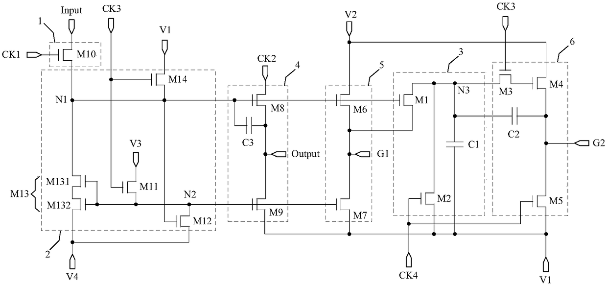
Embodiment 2

[0124] The first clock signal terminal CK1 and the fourth clock signal terminal CK4 can receive the same signal. The following description will be made by taking the first clock signal terminal CK1 and the fourth clock signal terminal CK4 both receiving the signal of the first clock signal terminal CK1 as an example.

[0125] Such as Figure 3b shown, select Figure 3b There are four stages in the circuit timing diagram shown: the first stage T1, the second stage T2, the third stage T3 and the fourth stage T4.

[0126] In the first stage T1, Input=1, CK1=1, CK2=0, CK3=0.

[0127] Since CK1=1, the second switch transistor M2 , the fifth switch transistor M5 and the tenth switch transistor M10 are all turned on. The turned-on tenth switch transistor M10 provides the high-level signal of the input signal terminal Input to the first node N1, so that the signal of the first node N1 is a high-level signal. Since the signal of the first node N1 is a high level signal, the first s...


PUM


Abstract

The invention discloses a shift register unit, a gate drive circuit, a display panel and a display device. The shift register unit comprises an input circuit, a first control circuit, a second controlcircuit, a cascade signal output circuit, a first scanning output circuit and a second scanning output circuit. Through mutual cooperation of the above six circuits, a cascade signal output end is allowed to output cascade signals to realize cascade shift trigger, a first scanning signal output end is allowed to output first scanning signals, a second scanning signal output end is allowed to output signal scanning signals, a certain phase difference is generated between the first scanning signals and the second scanning signals, each shift register unit is allowed to output two scanning signals with a certain shift difference to correspond two rows of gate lines in the display panel, the number of the shift register units in the gate drive circuit can be halved, occupation space of the gate drive circuit is reduced, and ultra-narrow border design is realized.

Description

technical field [0001] The invention relates to the field of display technology, in particular to a shift register unit, a gate drive circuit, a display panel and a display device. Background technique [0002] With the rapid development of display technology, the display panel is more and more developed towards the direction of high integration and low cost. Among them, the gate driver on array (Gate Driver on Array, GOA) technology integrates the thin film transistor (Thin Film Transistor, TFT) gate switching circuit on the array substrate of the display panel to form a scan drive for the display panel, so that the gate driver can be omitted. The wiring space of the Bonding area of ​​the integrated circuit (Integrated Circuit, IC) and the fan-out (Fan-out) area can not only reduce the product cost in terms of material cost and manufacturing process, but also make the display panel Beautiful design with symmetrical sides and narrow bezels. [0003] A general gate drive ci...

Claims


Application Information

Patent Timeline
Patent Type & Authority Applications(China)
IPC IPC(8): G09G3/36G11C19/28
CPCG09G3/3677G11C19/28
Inventor 陶健王迎唐锋景李红敏
Owner BOE TECH GRP CO LTD
Why Eureka
Try Eureka