
Micro-nano structured optical element and its preparation method and application

A micro-nano structure and optical element technology, applied in optical elements, optics, nanotechnology, etc., can solve problems such as increasing the transmission of blue-violet light, and achieve the effects of excellent mechanical strength, weather resistance, and low preparation cost.

Inactive Publication Date: 2020-11-17
苏州纳邦光电技术有限公司
View PDF5 Cites 0 Cited by
  • Summary
  • Abstract
  • Description
  • Claims
  • Application Information

AI Technical Summary

Problems solved by technology

The traditional three-dimensional micro-nano structure is a wide-spectrum anti-reflection and anti-reflection, which will also increase the transmission of blue-violet light.

Method used


Image

  • Micro-nano structured optical element and its preparation method and application
  • Micro-nano structured optical element and its preparation method and application
  • Micro-nano structured optical element and its preparation method and application

Examples


preparation example Construction

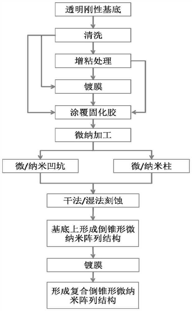
[0062] A specific process of the preparation method of the micro-nano structured optical element of the present invention is as follows: figure 1 As shown, the present invention provides a kind of preparation method of micro-nano structure optical element, comprises steps:

[0063] Step 1), providing a transparent rigid substrate.

[0064] As an example, step 1) further includes the steps of performing a cleaning process and an adhesion-increasing process on the transparent rigid substrate.

[0065] Preferably, the cleaning process includes one or a combination of two or more of a liquid phase cleaning process, a gas phase cleaning process and an ultraviolet light cleaning process.

[0066] Further, the gas phase cleaning process includes one of gas plasma cleaning and ozone cleaning, and the surface of the transparent rigid substrate is activated while cleaning, so as to improve the bonding force between the transparent rigid substrate and the subsequent process film.

[00...

Embodiment 1

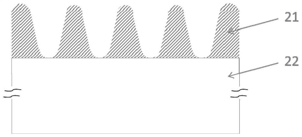
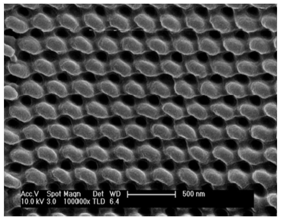
[0084] This embodiment provides a nanoimprinting method to prepare an inverted tapered micro-nano structure array on a sapphire cover plate, such as Figure 2a As shown, 21 is an array of inverted conical micro-nano structures, and 22 is a sapphire cover plate. This structure can achieve broad-spectrum anti-reflection and anti-reflection effects, and also has good mechanical strength and anti-wear performance. It has application prospects in lighting, display, showcase and other fields.

[0085] The following describes this embodiment in detail. The preparation method of the micro-nano structured optical element of this embodiment includes steps:

[0086] The first step: cleaning and surface treatment of the sapphire cover. Take a sapphire cover plate, put it into a mixed solution of concentrated sulfuric acid and hydrogen peroxide at a ratio of 3:1 at a temperature of 125 degrees Celsius, and clean it for 10 minutes. Subsequently, it was baked in an oven at 120 degrees Cel...

Embodiment 2

[0092] In this embodiment, the inverted conical micro-nano structure array is combined with the coating to form a composite inverted conical micro-nano structure array on the sapphire cover plate, such as Figure 3a shown, where 31 is SiO 2 The coating layer has an array of inverted conical micro-nano structures, and 32 is a sapphire cover plate. The structure can achieve broad-spectrum anti-reflection and anti-reflection effects, and at the same time has a certain inhibitory effect on the transmission of blue-violet light, and has application prospects in lighting, display and other fields.

[0093] The following describes this embodiment in detail. The preparation method of the micro-nano structured optical element of this embodiment includes steps:

[0094] The first step: cleaning and surface treatment of the sapphire cover. Take a sapphire cover plate, put it into a mixed solution of concentrated sulfuric acid and hydrogen peroxide at a ratio of 3:1 at a temperature of ...


PUM

PropertyMeasurementUnit
sizeaaaaaaaaaa
sizeaaaaaaaaaa
depthaaaaaaaaaa

Abstract

The invention provides a micro-nanostructure optical element and a preparation method and application thereof. The micro-nanostructure optical element is characterized by forming an inverted-cone-shaped micro-nano structure array on a transparent rigid base. The micro-nanostructure optical element not only has broadband-spectrum wide-angle antireflection properties, but also has higher mechanicalstrength. The micro-nanostructure optical element can be combined with one or more layers of materials with different optical refractive indexes, and realizes a selective wide-spectrum wide-angle anti-reflection effect for the incident light. Based on gradient index of a 3D nanostructure, the mechanical stability of the inverted-cone-shaped structure and spectrum adjustment of optical filming, themethod can obtain the micro-nanostructure optical element having selective wide-spectrum wide-angle anti-reflection properties and higher mechanical strength. The novel optical element has a wide application prospect in the illumination, display, thermoelectricity, photocatalysis and photovoltaic fields and the like.

Description

technical field [0001] The invention relates to the technical field of micro-processing and manufacturing, in particular to a micro-nano structured optical element and its preparation method and application. Background technique [0002] Anti-reflection and anti-reflection coatings are widely used in lighting, display, microlens, photovoltaic, showcase glass and other fields due to their excellent optical properties. The conventional antireflection and antireflection coating preparation method is to deposit a certain thickness of low refractive index material (such as silicon dioxide, silicon nitride and magnesium fluoride, etc.) on the surface of the device. This kind of anti-reflection coating uses the principle of interference extinction, and often can only suppress the reflection of a narrower band. If a broad-spectrum anti-reflection and anti-reflection effect is required, multi-layer films of different thicknesses and material systems need to be deposited, resulting i...

Claims


Application Information

Patent Timeline
Patent Type & Authority Patents(China)
IPC IPC(8): G02B1/118B82Y40/00B82Y30/00
CPCB82Y30/00B82Y40/00G02B1/118
Inventor 林引岳楼成飞张培俊葛勤
Owner 苏州纳邦光电技术有限公司
Learn More