DIP16 multichip packaging special lead frame and packaging method thereof

A multi-chip packaging, special-shaped lead technology, applied in electrical components, electrical solid devices, circuits, etc., can solve the problems of single structure and large upper board area, so as to reduce the damage to the device, reduce the area, and improve the working stability. Effect

Active Publication Date: 2018-07-06
四川明泰微电子科技股份有限公司
View PDF9 Cites 0 Cited by
  • Summary
  • Abstract
  • Description
  • Claims
  • Application Information

AI Technical Summary

Problems solved by technology

[0004] Aiming at the defects of single structure and large board area after the current control system is integrated in the prior art, the present invention discloses a special-shaped lead frame for DIP16 multi-chip packaging and its packaging method. The lead frame of the present invention passes through multiple base islands It not only realizes the integration of multiple MOS tubes, but also reduces the mutual interference between the devices, improves the working stability, and at the same time better realizes the control of the current, and also greatly reduces the packaging cost and device work damage

Method used


Image

  • DIP16 multichip packaging special lead frame and packaging method thereof
  • DIP16 multichip packaging special lead frame and packaging method thereof

Examples


Embodiment 1

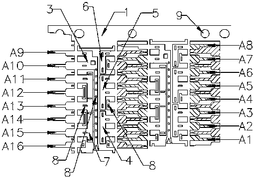
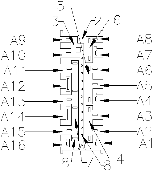
[0032] This embodiment, as a preferred embodiment of the present invention, discloses a DIP16 multi-chip packaging special-shaped lead frame, and its specific structure is as follows: figure 1 As shown, it includes a lead frame body, and a plurality of frame units are arranged in the lead frame body, the first to eighth pins are arranged on one side of the frame unit in turn, and the ninth pins are arranged in turn on the other side of the frame unit. To the sixteenth pin, a long base island is provided in the middle of the frame unit, and a circular locking glue hole is provided on the long base island; one end of the long base island is connected to the ninth and tenth pins; the The first to third base islands are arranged on the side of the long base island close to the first to eighth pins; the first base island is connected to the second and third pins, and the second base island is connected to the fifth and third pins. The six pins are connected, the third base island i...

Embodiment 2

[0035] According to a kind of DIP16 multi-chip packaging special-shaped lead frame described in embodiment 1, the present invention also provides the packaging method of this lead frame, comprises the following steps:

[0036] A. First paste 3 MOS chips numbered a, b, and c with the same structure on the fourth base island, and then paste the chips on the first, second and third base islands in sequence. The chip numbers are f in turn , e, d, after the pasting is completed, send it to the oven for pre-curing baking. The pre-curing baking is at a constant temperature of 170°C, and a protective nitrogen gas is introduced. The nitrogen flow rate is greater than 40L / MIN, and the baking time is 1 hour;

[0037]B. First connect the S poles of chips a, b, and c to the first base island, the second base island, and the third base island respectively through wires; then connect the S poles of chips d, e, and f to the Connect the long base island; then connect the G pole of chip a to th...

Embodiment 3

[0046] According to a kind of DIP16 multi-chip packaging special-shaped lead frame described in embodiment 1, the present invention also provides the packaging method of this lead frame, comprises the following steps:

[0047] A. First paste 3 MOS chips numbered a, b, and c with the same structure on the fourth base island, and then paste the chips on the first, second and third base islands in sequence. The chip numbers are f in turn , e, d, after the paste is completed, send it to the oven for pre-curing baking. The pre-curing baking is at a constant temperature of 175°C, and the protective nitrogen gas is introduced. The nitrogen flow rate is greater than 40L / MIN, and the baking time is 1 hour;

[0048] B. First connect the S poles of chips a, b, and c to the first base island, the second base island, and the third base island respectively through wires; then connect the S poles of chips d, e, and f to the Connect the long base island; then connect the G pole of chip a to t...


PUM


Abstract

The invention discloses a DIP16 multichip packaging special lead frame machine packaging method. A lead frame body is included; the lead frame body is provided with multiple frame units; one side of the frame unit is provided with pins from a first to an eighth, and the other side is provided with pins from a ninth to a sixteenth; a long base island is also arranged on the frame unit; two sides ofthe long base island are provided with base islands from a first to a fourth; and chips are attached to the base islands from the first to the fourth. Through integrating multiple MOS transistors onthe same chip and realizing switching of positive and negative electric signals and switching of strong and weak electric signals through external lines, the area of an integrated circuit board can beeffectively reduced in the case of system integration, and miniaturization of the integrated circuit is thus realized.

Description

technical field [0001] The invention relates to the technical field of integrated circuit packaging equipment, in particular to a special-shaped lead frame for DIP16 multi-chip packaging and a packaging method thereof. Background technique [0002] DIP (Dual Inline Package) package chip refers to an integrated circuit chip that is packaged in a dual-inline package, and most small and medium-sized integrated circuits (ICs) use this package. A CPU chip in a DIP package usually has two rows of pins, which are soldered and mounted by direct insertion into a chip socket with a DIP structure or directly on a circuit board with the same number of solder holes and geometric arrangement. At present, DIP package lead frames in the industry are mainly single-base island lead frames. The main defect of single-base island lead frames is that they have a single structure and cannot be used for multi-purpose, medium and large-scale system integration devices. , several or even a dozen dev...

Claims


Application Information

Patent Timeline
Patent Type & Authority Applications(China)
IPC IPC(8): H01L23/495H01L21/60H01L25/07
CPCH01L23/49503H01L23/49562H01L24/83H01L24/85H01L25/072H01L2224/832H01L2224/852
Inventor 李蛇宏杨益东
Owner 四川明泰微电子科技股份有限公司
Why Eureka
Try Eureka