Eureka AIR delivers breakthrough ideas for toughest innovation challenges, trusted by R&D personnel around the world.

Luminescent material and preparation method thereof and semiconductor device

A technology of luminescent materials and semiconductors, applied in the field of quantum dots, can solve the problems that cannot meet the requirements of luminescent materials of semiconductor devices, and the luminous performance needs to be improved, so as to achieve the effect of meeting the comprehensive performance requirements and high luminous efficiency

Pending Publication Date: 2018-07-10
TCL CORPORATION
View PDF3 Cites 2 Cited by
  • Summary
  • Abstract
  • Description
  • Claims
  • Application Information

AI Technical Summary

Problems solved by technology

[0013] In view of the above deficiencies in the prior art, the object of the present invention is to provide a luminescent material, a preparation method and a semiconductor device, aiming to solve the problem that the luminescent performance of the existing luminescent material needs to be improved and cannot meet the requirements of the semiconductor device for the luminescent material

Method used


Image

  • Luminescent material and preparation method thereof and semiconductor device
  • Luminescent material and preparation method thereof and semiconductor device
  • Luminescent material and preparation method thereof and semiconductor device

Examples


Embodiment 1

[0100] Embodiment 1: Preparation based on CdZnSeS / CdZnSeS quantum dots

[0101] The precursors of cation Cd, cation Zn, anion Se and anion S are injected into the reaction system to form Cd y Zn 1-y Se b S 1-b Layer (where 0≤y≤1, 0≤b≤1); continue to inject the precursors of cation Cd, cation Zn, anion Se and anion S into the reaction system, in the above Cd y Zn 1-y Se b S 1-b Cd z Zn 1-z Se c S 1-c layer (where 0≤z≤1, and z is not equal to y, 0≤c≤1); under certain reaction conditions such as heating temperature and heating time, Cd and The exchange of Zn ions; because the migration distance of cations is limited and the probability of migration is smaller the farther the migration distance is, so it will be in Cd y Zn 1-y Se b S 1-b layer with Cd z Zn 1-z Se c S 1-c A graded alloy composition distribution of Cd content and Zn content is formed near the interface of the layer, that is, Cd x Zn 1-x Se a S 1-a , where 0≤x≤1, 0≤a≤1.

Embodiment 2

[0102] Embodiment 2: Preparation based on CdZnS / CdZnS quantum dots

[0103] The precursors of cation Cd, cation Zn and anion S are injected into the reaction system to form Cd y Zn 1-y S layer (where 0≤y≤1); continue to inject the precursor of cation Cd, the precursor of cation Zn and the precursor of anion S into the reaction system, the above Cd y Zn 1-y Cd formed on the surface of the S layer z Zn 1-z S layer (where 0≤z≤1, and z is not equal to y); under certain reaction conditions such as heating temperature and heating time, the exchange of Cd and Zn ions in the inner and outer nanocrystals (that is, the above two-layer compound) occurs ; Since the migration distance of cations is limited and the farther the migration distance is, the probability of migration is smaller, so the Cd y Zn 1-y S layer and Cd z Zn 1-z A gradual alloy composition distribution of Cd content and Zn content is formed near the interface of the S layer, that is, Cd x Zn 1-x S, where 0≤x≤1....

Embodiment 3

[0104] Embodiment 3: Preparation based on CdZnSe / CdZnSe quantum dots

[0105] The precursors of cation Cd, cation Zn and anion Se are injected into the reaction system first to form Cd y Zn 1-y Se layer (where 0≤y≤1); continue to inject the precursor of cation Cd, the precursor of cation Zn and the precursor of anion Se into the reaction system, the above Cd y Zn 1-y Cd formed on the surface of the Se layer z Zn 1-z Se layer (where 0≤z≤1, and z is not equal to y); under certain reaction conditions such as heating temperature and heating time, the exchange of Cd and Zn ions in the inner and outer nanocrystals occurs; due to the limited migration distance of cations And the farther the migration distance is, the smaller the probability of migration will be, so it will be in Cd y Zn 1-y Se layer and Cd z Zn 1-z A graded alloy composition distribution of Cd content and Zn content is formed near the interface of the Se layer, that is, Cd x Zn 1-x Se, where 0≤x≤1.


PUM


Abstract

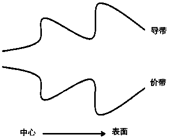
The invention discloses a luminescent material and a preparation method thereof and a semiconductor device. The luminescent material comprises N(N is greater than 1) luminescent units sequentially arranged along a radial direction; the luminescent units are of gradient alloy component structure of which outer level width is reduced gradually from inside to outside in the radial direction; energy levels of adjacent luminescent units are not discontinuous. The novel luminescent material is of the alloy component changing gradually from inside to outside along the radial direction, not only realizes efficient luminous efficiency, but can meet comprehensive performance requirements from the semiconductor device and corresponding display technology, and is an ideal luminescent material suitablefor the semiconductor device and the corresponding display technology.

Description

technical field [0001] The invention relates to the field of quantum dots, in particular to a luminescent material, a preparation method and a semiconductor device. Background technique [0002] Quantum dots are a special material that is confined to the order of nanometers in three dimensions. This remarkable quantum confinement effect makes quantum dots have many unique nanometer properties: continuously adjustable emission wavelength, narrow emission wavelength, Broad absorption spectrum, high luminous intensity, long fluorescence lifetime and good biocompatibility, etc. These characteristics make quantum dots have broad application prospects in flat panel display, solid state lighting, photovoltaic solar energy, biomarkers and other fields. Especially in flat panel display applications, quantum dot light-emitting diodes (Quantum dot light-emitting diodes, QLEDs) based on quantum dot materials have made great progress in display image quality, device performance, and man...

Claims


Application Information

Patent Timeline
Patent Type & Authority Applications(China)
IPC IPC(8): C09K11/88C09K11/56C09K11/02B82Y20/00B82Y30/00B82Y40/00H01L51/50
CPCC09K11/02C09K11/565C09K11/883B82Y20/00B82Y30/00B82Y40/00H10K50/115
Inventor 杨一行刘政钱磊程陆玲
Owner TCL CORPORATION
Why Eureka
Eureka Blog
Learn More