Microcosmic and nano-scale electro-mechanical coupling feature measurement device based on AFM and detection method thereof

A technology of measuring device and measuring method, which is applied in the measurement of the change force of the optical properties of the material when it is stressed, and the resistance of the material, which can solve the problems of difficult operation technology, impossible test, difficult operation, scientific research workers, etc. question

Active Publication Date: 2018-07-17
常州市利多合金材料有限公司 +1
View PDF14 Cites 3 Cited by
  • Summary
  • Abstract
  • Description
  • Claims
  • Application Information

AI Technical Summary

Problems solved by technology

For example, the patent "Mechanical-Electric Coupling Effect Test System and Its Test Method for Conductive Functional Materials" with application number 201510303120.3 can realize the force-electricity coupling test during the dynamic change process of macroscopic conductive materials. Coupled testing cannot be done at this stage
For example, the application number 201520896619.5 "A Device for In-Situ Micromechanics, Microstructure, and Component Integration Research in Scanning Electron Microscope" can realize the research on micromechanics and microstructure with high test accuracy and low interference to scanning electron microscope imaging , but the device is complex and the cost of the device is high, and the operation technology is difficult
The current equipment and methods are still unable to achieve real-time measurement of microstructure and the cost of testing is high, the structure of the device is complex, and the operation is difficult. Problems have also plagued scientific researchers.

Method used


Image

  • Microcosmic and nano-scale electro-mechanical coupling feature measurement device based on AFM and detection method thereof
  • Microcosmic and nano-scale electro-mechanical coupling feature measurement device based on AFM and detection method thereof
  • Microcosmic and nano-scale electro-mechanical coupling feature measurement device based on AFM and detection method thereof

Examples


Embodiment Construction

[0039] The present invention will be further described below in conjunction with the accompanying drawings and specific embodiments, but the protection scope of the present invention is not limited thereto.

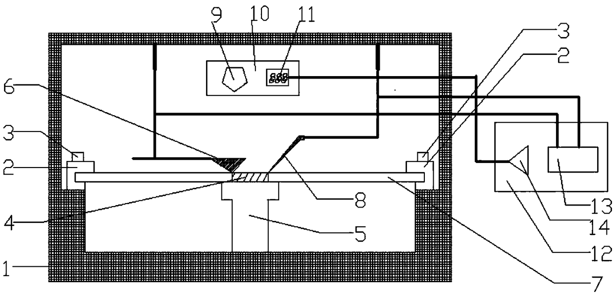
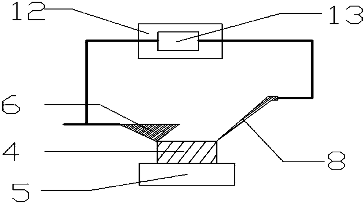
[0040] like figure 1 and figure 2As shown, the AFM-based micro / nano force-electric coupling characteristic measuring device of the present invention includes a piezoelectric driver 5, an AFM probe 6, a conductive second probe 8, a laser emitter 9, an AFM atomic force microscope 10, Detector 11 and data processing center 12; the two ends of the flexible elastic conductive sample 7 are installed on the fixed frame 1 through the clamp 2 and clamped with the nut 3; the movable piezoelectric driver 5 is installed on the fixed frame 1, and the The piezoelectric driver 5 is located on the bottom surface of the flexible elastic conductive sample 7; the AFM probe 6 and the second conductive probe 8 are installed on the fixed frame 1, and the AFM probe 6 is in contact with the su...


PUM

PropertyMeasurementUnit
sizeaaaaaaaaaa

Abstract

The present invention provides a microcosmic and nano-scale electro-mechanical coupling feature measurement device based on an AFM (Atomic Force Microscope). The device comprises a piezoelectric actuator, an AFM probe, a conductive second probe, a laser emitter, a microscope, a detector and a data processing center; two ends of a flexible and elastic conductive sample are installed on a fixed mount through clamps; the movable piezoelectric actuator is installed on the fixed mount; the fixed mount is provided with the AFM probe and the conductive second probe, the AFM probe is in contact with the surface of the flexible and elastic conductive sample through motion, and the conductive second probe is in contact with the surface of the flexible and elastic conductive sample; and an AFM is internally provided with the laser emitter and the detector, and the laser emitter is configured to emit signals. The microcosmic and nano-scale electro-mechanical coupling feature measurement device based on the AFM and the detection method thereof can perform test of the nano-scale conductive performance and mechanical load coupling relation so as to dynamically reflect the relation of the mechanical loads, the structures and the material performances of test samples under the electro-mechanical coupling action in real time.

Description

technical field [0001] The invention relates to the field of flexible elastic conductive composite materials and strain sensing networks, in particular to an AFM-based micro / nano force-electric coupling characteristic measuring device and method thereof. Background technique [0002] The nano-measurement technology represented by AFM is an important part of the nano-measurement technology. Nanotechnology is to change the material structure within the scale range of 1-100nm through certain instruments and equipment, so as to reflect the material properties that macroscopic bulk materials do not have in many aspects such as physics and chemistry. With the rapid development of nanotechnology in recent years, new nano-characterization technologies that support the development of nanotechnology have emerged in an endless stream. In addition, the development of physical and chemical preparation technology has also led to the continuous emergence of a large number of advanced nano...

Claims


Application Information

Patent Timeline
Patent Type & Authority Applications(China)
IPC IPC(8): G01L1/24G01N27/04
CPCG01L1/24G01N27/04
Inventor 王学森王成原张康俞笑竹赵越孙虎
Owner 常州市利多合金材料有限公司
Why Eureka
Try Eureka