OLED substrate and preparation method thereof and display device

A technology for substrates and display areas, which is applied in semiconductor/solid-state device manufacturing, semiconductor devices, electrical components, etc., and can solve problems such as poor uniformity of organic layer thickness

Active Publication Date: 2018-07-27
BOE TECH GRP CO LTD
View PDF9 Cites 8 Cited by
  • Summary
  • Abstract
  • Description
  • Claims
  • Application Information

AI Technical Summary

Problems solved by technology

[0003] In the actual inkjet printing process, it is found that the drying rate of the organic solvent in the edge area will be faster than th

Method used


Image

  • OLED substrate and preparation method thereof and display device
  • OLED substrate and preparation method thereof and display device
  • OLED substrate and preparation method thereof and display device

Examples


Embodiment Construction

[0026] The following will clearly and completely describe the technical solutions in the embodiments of the present invention with reference to the accompanying drawings in the embodiments of the present invention. Obviously, the described embodiments are only some, not all, embodiments of the present invention. Based on the embodiments of the present invention, all other embodiments obtained by persons of ordinary skill in the art without making creative efforts belong to the protection scope of the present invention.

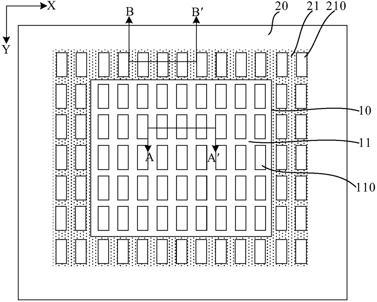
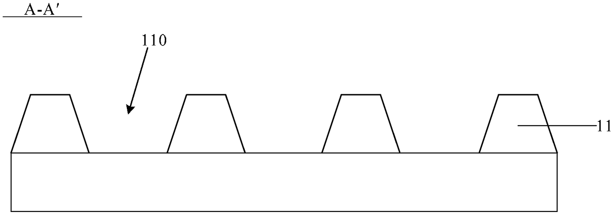
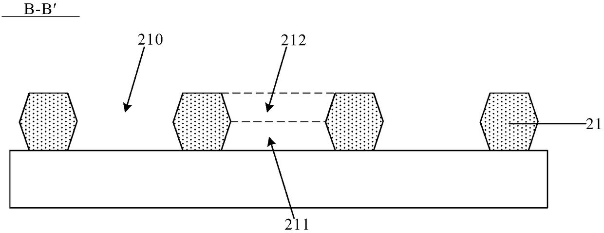
[0027] An embodiment of the present invention provides an OLED substrate, such as figure 1 As shown, it includes: a display area 10 and a non-display area 20, and the non-display area 20 includes a virtual pixel area ( figure 1 not marked in); the display area 10 includes a first pixel defining layer 11 disposed on the substrate, and the first pixel defining layer 11 includes a plurality of first openings 110 corresponding to the sub-pixels one by one; the dum...


PUM


Abstract

The embodiment of the invention provides an OLED substrate and a preparation method thereof and a display device, and relates to the technical field of display, and the film thickness uniformity of organic layers of sub-pixels of an edge area and an intermediate area in a display area can be improved. The OLED substrate comprises the display area and a non-display area, and the non-display area comprises a virtual pixel area arranged around the display area; the display area comprises a first pixel defining layer arranged on a substrate, and the first pixel defining layer includes a pluralityof first openings corresponding to the sub-pixels one by one; the virtual pixel area includes a second pixel defining layer arranged on the substrate, and the second pixel defining layer includes a plurality of second openings corresponding to the sub-pixels one by one; the volume of the second openings is greater than the volume of the first openings, and the area of the upper surfaces, away fromthe substrate, of the second openings is smaller than or equal to the area of the upper surfaces, away from the substrate, of the first openings.

Description

technical field [0001] The invention relates to the field of display technology, in particular to an OLED substrate, a preparation method thereof, and a display device. Background technique [0002] In an organic light-emitting diode (Organic Light-Emitting Diode, OLED) display substrate, an OLED device includes an anode, at least one organic layer, a cathode, and the like. Wherein, at least one organic layer may be one or more layers of light emitting layer, hole transport layer, electron transport layer, hole injection layer and electron injection layer. When using an inkjet printing process to form an organic layer, it is necessary to first form a pixel defining layer on a substrate, and then print an organic solvent into the openings of the pixel defining layer. [0003] In the actual inkjet printing process, it is found that the drying rate of the organic solvent in the edge area is faster than that in the middle area, resulting in poor film thickness uniformity of the...

Claims


Application Information

Patent Timeline
IPC IPC(8): H01L27/32H01L51/56
CPCH10K71/135H10K59/122H10K71/00H10K59/88H10K59/1201
Inventor 胡春静侯文军
Owner BOE TECH GRP CO LTD
Why Eureka
Try Eureka