Electroluminescence device and its light-emitting layer and application
A technology for electroluminescent devices and light-emitting layers, which can be used in electro-solid devices, electrical components, semiconductor devices, etc., and can solve problems such as luminous efficiency gaps
- Summary
- Abstract
- Description
- Claims
- Application Information
AI Technical Summary
Problems solved by technology
Method used
Image

Examples
Embodiment 1
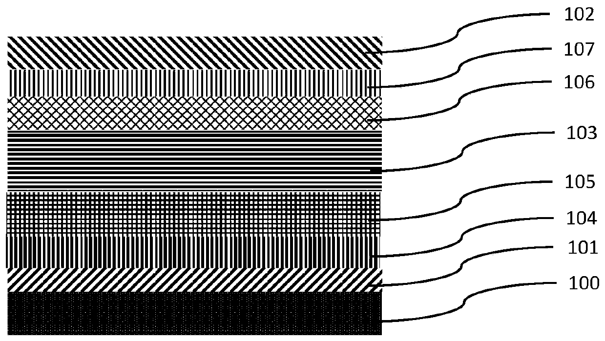
[0061] The present embodiment is an electroluminescence device, the structure is:
[0062] ITO / PEDOT:PSS / PVK / PO-T2T:mCP:(CdSe / ZnSquantum dot) / PO-T2T / LiF / Al.
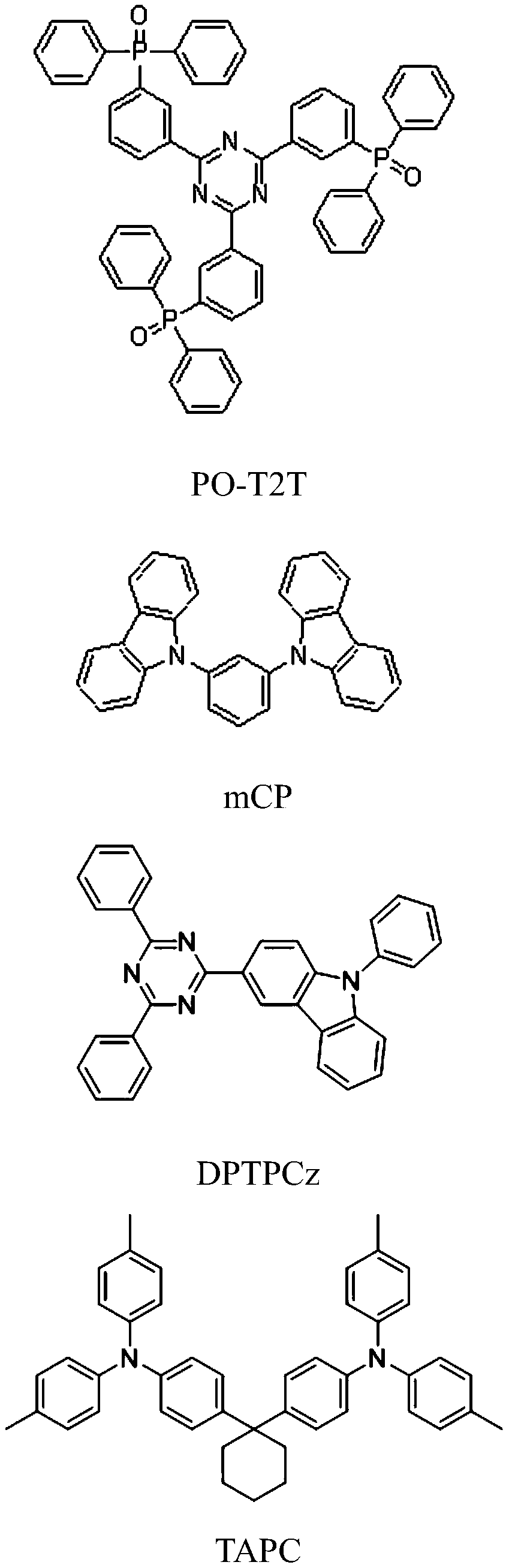
[0063] Among them, PO-T2T (triplet state energy level 2.99eV) and mCP (triplet state energy level 2.94eV) are used as organic materials in the light-emitting layer to form a delayed fluorescence exciplex (triplet state energy level is about 2.64eV, and the emission spectrum is in the blue light band);
[0064] Using (CdSe / ZnS quantum dot) as the nanocrystalline semiconductor material, the excitation spectrum covers the band from ultraviolet to green light, and the emission spectrum is in the red band;
[0065] The decay lifetime of the excited state of the exciplex (about 500 ns) is 10 times that of the excited state of the nanocrystalline semiconductor material (about 50 ns).
[0066] The preparation steps of the above-mentioned electroluminescent device are as follows:
[0067](1) Substrate treatment: Clean the surf...
Embodiment 2
[0077] The present embodiment is an electroluminescence device, the structure is:
[0078] ITO / PEDOT:PSS / PVK / PO-T2T:mCP:(CdSe / ZnSquantum rod) / PO-T2T / LiF / Al.
[0079] Among them, PO-T2T (triplet state energy level 2.99eV) and mCP (triplet state energy level 2.94eV) are used as organic materials in the light-emitting layer to form a delayed fluorescence exciplex (triplet state energy level is about 2.64eV, and the emission spectrum is in the blue light band);
[0080] Using (CdSe / ZnS quantum rod) as a nanocrystalline semiconductor material, the excitation spectrum covers the wavelength band from ultraviolet to green light, and the emission spectrum is in the red light band;
[0081] The decay lifetime (about 500 ns) of the excited state of the exciplex is 25 times the decay lifetime (about 20 ns) of the excited state of the quantum rod of the nanocrystalline semiconductor material.
[0082] The preparation of the above electroluminescent device is similar to that of Example 1,...
Embodiment 3
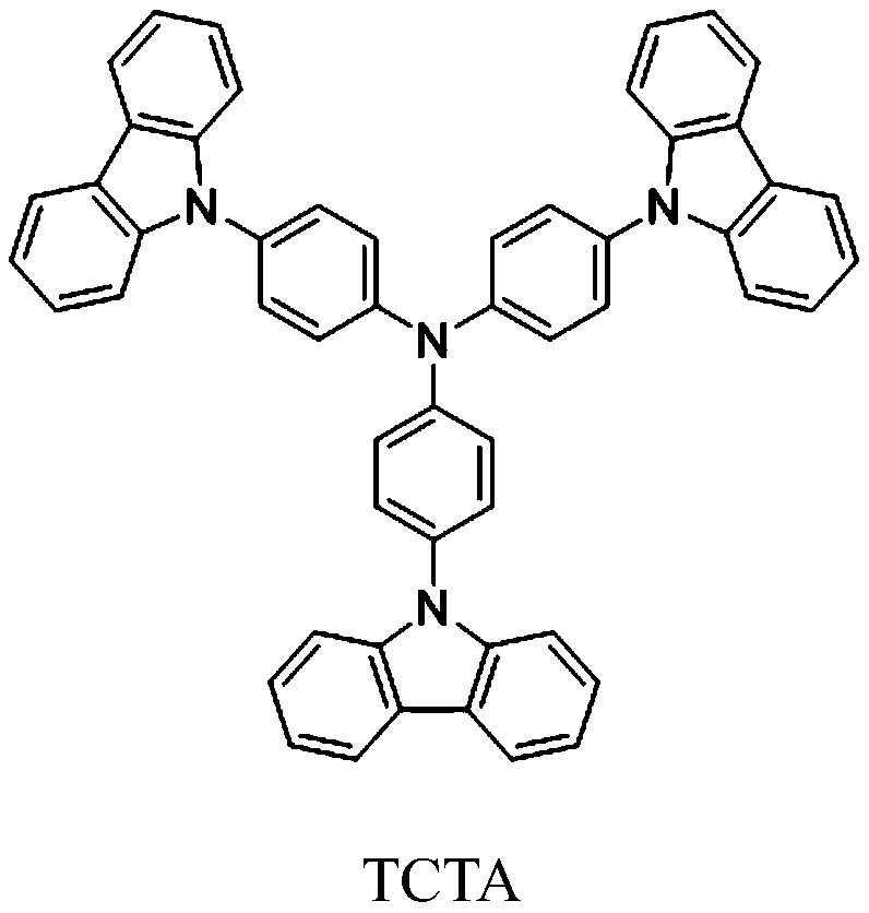
[0084] The present embodiment is an electroluminescence device, the structure of which is: ITO / PEDOT:PSS / PVK / DPTPCz:TAPC:(CdSe / ZnS quantum dot) / PO-T2T / LiF / Al.
[0085] Among them, the light-emitting layer uses DPTPCz (triplet energy level 2.77eV) and TAPC (triplet energy level 2.91eV) as organic materials to form a delayed fluorescence exciplex (triplet energy level 2.47eV, emission spectrum in the green band) ;
[0086] Using (CdSe / ZnS quantum dot) as the nanocrystalline semiconductor material, the excitation spectrum covers the band from ultraviolet to green light, and the emission spectrum is in the red band;
[0087] The decay lifetime of the excited state of the exciplex (about 2 μs) is 40 times that of the excited state of the nanocrystalline semiconductor material (about 50 ns).
[0088] The preparation steps of the above-mentioned electroluminescent device are as follows:
[0089] (1) Substrate treatment: Clean the surface of the substrate with glass cleaner and pure...
PUM
 Abstract
Description
Claims
Application Information
 - R&D
- Intellectual Property
- Life Sciences
- Materials
- Tech Scout
- Unparalleled Data Quality
- Higher Quality Content
- 60% Fewer Hallucinations
Browse by: Latest US Patents, China's latest patents, Technical Efficacy Thesaurus, Application Domain, Technology Topic, Popular Technical Reports.
© 2025 PatSnap. All rights reserved.Legal|Privacy policy|Modern Slavery Act Transparency Statement|Sitemap|About US| Contact US: help@patsnap.com