
Image sensor and method of forming the same

An image sensor and filter technology, used in semiconductor devices, electrical solid state devices, radiation control devices, etc., can solve the problems of underexposure, insufficient dynamic range of the image sensor, overexposure of the output image, etc., to prolong the exposure time, improve the Image quality, the effect of improving the dynamic range

Active Publication Date: 2021-03-02
淮安西德工业设计有限公司
View PDF5 Cites 0 Cited by
  • Summary
  • Abstract
  • Description
  • Claims
  • Application Information

AI Technical Summary

Problems solved by technology

[0006] However, in the prior art, the dynamic range of the image sensor is often insufficient, and the output image is prone to overexposure or underexposure.

Method used


Image

  • Image sensor and method of forming the same
  • Image sensor and method of forming the same
  • Image sensor and method of forming the same

Examples


Embodiment Construction

[0028] In the prior art, the optical filter matrix includes a plurality of minimum repeating units, and the optical filter matrix may be, for example, a Bayer array, a mosaic sequential array or other pattern arrays.

[0029] In the filter matrix, more green filters are generally arranged, so in order to improve the image quality output by the image sensor, the photoelectric response performance of the green filter should be improved as much as possible. Taking the Bayer array as an example, the green filter contained in the minimum repeating unit is twice as many as the red filter or the blue filter, and the green filter is alternately embedded in the adjacent row between the blue filter between or between red filters.

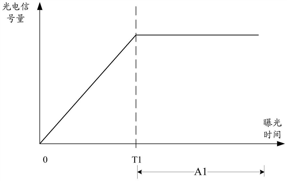
[0030] figure 1 It is a schematic diagram of a photoelectric response curve of a green filter of an image sensor in the prior art.

[0031] like figure 1 As shown, the horizontal axis is the exposure time under a fixed light intensity environment, the long...


PUM

PropertyMeasurementUnit
thicknessaaaaaaaaaa
thicknessaaaaaaaaaa

Abstract

An image sensor and its forming method, the image sensor includes: a semiconductor substrate; a pixel device located in the semiconductor substrate; a filter matrix located on the surface of the semiconductor substrate, each of the filter The filter matrix includes a plurality of minimum repeating units, and the minimum repeating unit includes at least a first green filter and a second green filter, and the thickness of the first green filter is different from that of the second green filter . The solution of the invention can improve the dynamic range of the image sensor.

Description

technical field [0001] The invention relates to the technical field of semiconductor manufacturing, in particular to an image sensor and a forming method thereof. Background technique [0002] The image sensor is the core component of the camera equipment, which realizes the image capture function by converting the optical signal into an electrical signal. Taking a CMOS image sensor (CMOS Image Sensors, CIS) device as an example, due to its advantages of low power consumption and high signal-to-noise ratio, it has been widely used in various fields. [0003] Taking Back-side Illumination (BSI for short) CIS as an example, in the existing manufacturing process, logic devices, pixel devices and metal interconnection structures are first formed in the semiconductor substrate, and then the carrier wafer and the described The front side of the semiconductor substrate is bonded, and then the back of the semiconductor substrate is thinned, and the subsequent process of forming a C...

Claims


Application Information

Patent Timeline
Patent Type & Authority Patents(China)
IPC IPC(8): H01L27/146
CPCH01L27/14625H01L27/14685
Inventor 吕相南北村陽介黄晓橹
Owner 淮安西德工业设计有限公司
Learn More