Touch control display substrate, manufacturing method therefor, and display device

A technology for a touch display substrate and a manufacturing method, which is applied in semiconductor/solid-state device manufacturing, instrumentation, electrical digital data processing, etc., and can solve problems such as low light transmittance, thick display device, large display area and touch blind area, etc. Achieve the effect of improving touch precision, realizing narrow frame and large size, and ensuring uniform design

Inactive Publication Date: 2018-08-03
BOE TECH GRP CO LTD
View PDF5 Cites 12 Cited by
  • Summary
  • Abstract
  • Description
  • Claims
  • Application Information

AI Technical Summary

Problems solved by technology

However, this technology has disadvantages such as low light transmittance and thicker display devices.
[0004] In order to reduce the thickness of the OLED touch display device, the prior art proposes a scheme in which the cathode of the OLED touch display device is multiplexed as a touch electrode. The common layer is below the cathode. Since it is not easy to form a via hole through the common layer, therefore , the touch electrodes are all connected to the touch signal lines

Method used


Image

  • Touch control display substrate, manufacturing method therefor, and display device
  • Touch control display substrate, manufacturing method therefor, and display device
  • Touch control display substrate, manufacturing method therefor, and display device

Examples


Embodiment Construction

[0061] In order to make the technical problems, technical solutions and advantages to be solved by the embodiments of the present invention clearer, the following will describe in detail with reference to the drawings and specific embodiments.

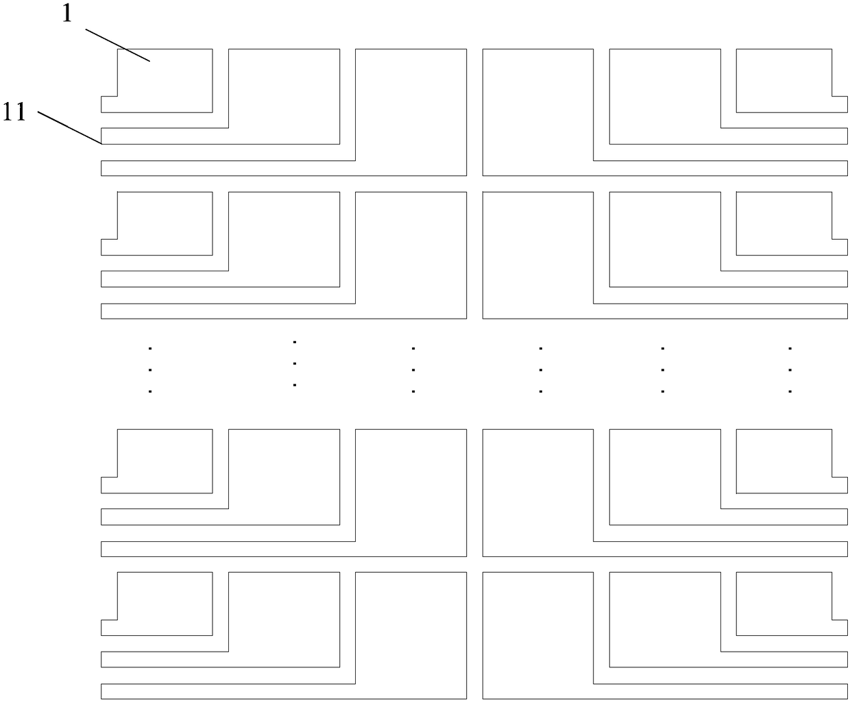
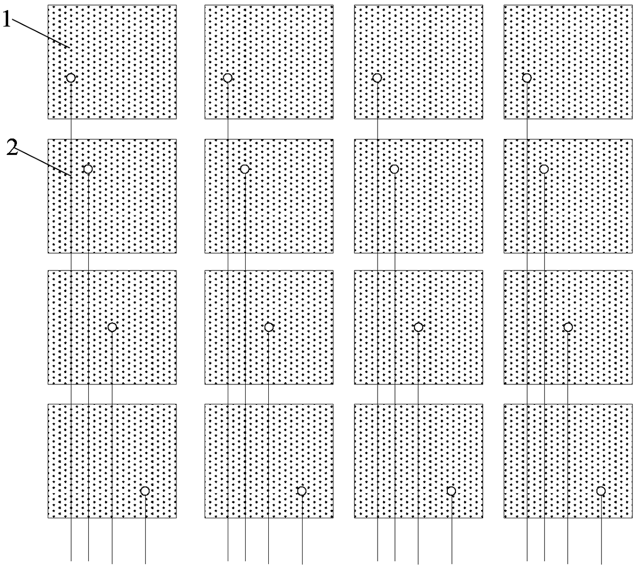
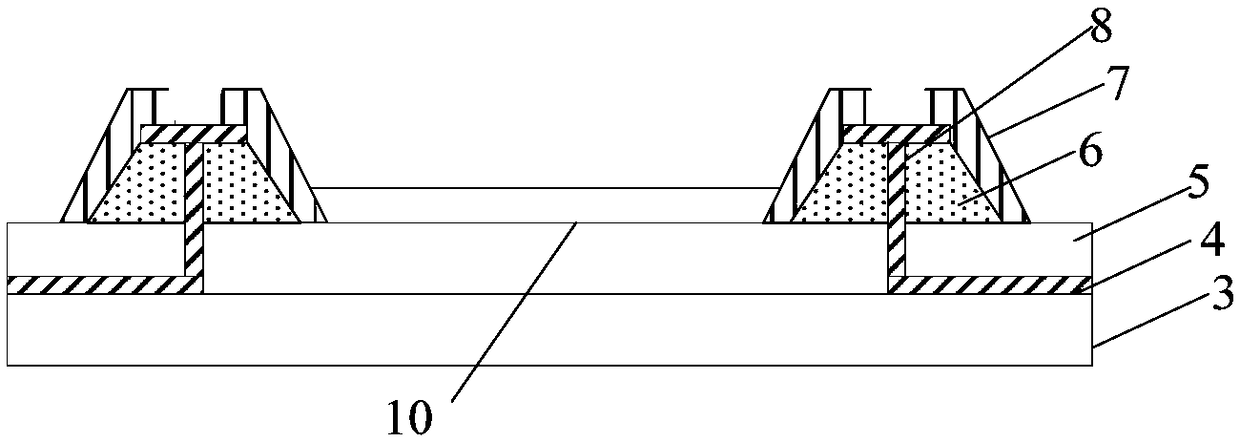
[0062] In the prior art, in order to reduce the thickness of the OLED touch display device, the cathode of the OLED touch display device is multiplexed as a touch electrode, but since it is difficult to form a via hole penetrating through the common layer, as figure 1 As shown, the touch electrodes 1 are all led to the periphery of the display area through traces 11, and then connected to the touch signal lines below the common layer through vias located around the display area. In the wiring area, as the size of the touch display device increases and the number of touch electrodes increases, the area of ​​the surrounding wiring area will also increase, resulting in a relatively large touch blind area around the display area, which is n...


PUM


Abstract

The invention provides a touch control display substrate, a manufacturing method therefor and a display device, and belongs to the technical field of touch control display. The manufacturing method comprises the steps: sequentially forming an anode, a common layer and touch control electrodes on a substrate; forming touch control signal lines and conductive connecting lines in a display region ofthe touch control display substrate, wherein the touch control signal lines are corresponding to touch control electrodes in a one-to-one manner, and are electrically connected with the correspondingtouch control electrodes through the conductive connecting lines. According to the technical scheme of the invention, the method can achieve the narrow frame and big size of an embedded touch controldisplay device.

Description

technical field [0001] The present invention relates to the technical field of touch display, in particular to a touch display substrate, a manufacturing method thereof, and a display device. Background technique [0002] With the rapid progress of display technology, organic light emitting diode (Organic Light Emitting Diode, OLED), which is the core semiconductor element technology of the display device, has also been greatly improved. For existing display devices, OLED, as a current-mode light-emitting device, is increasingly used in In the field of high-performance display. [0003] With the development of portable electronic display devices, touch display devices provide a new human-computer interaction interface, which is more direct and humanized in use. Currently, the OLED touch display device is usually made by separating the OLED display screen and the touch screen, and then combining the two. The OLED touch display device generally includes an OLED substrate, a...

Claims


Application Information

Patent Timeline
IPC IPC(8): H01L27/32H01L21/77G06F3/041
CPCG06F3/041H01L21/77H10K59/12H10K59/131G06F3/0412G06F3/04164G06F3/0443G06F2203/04103H01L27/124H10K59/40H10K59/122H10K71/00H10K59/1201
Inventor 杨盛际董学陈小川王辉王晏酩于芳李伟
Owner BOE TECH GRP CO LTD
Why Eureka
Try Eureka