Unlock instant, AI-driven research and patent intelligence for your innovation.

Thin film transistor (TFT), preparation method thereof and display device

A thin-film transistor and semiconductor technology, applied in transistors, electric solid-state devices, semiconductor devices, etc., can solve the problem of small capacitance of passivation layer, and achieve the effect of reducing power consumption, high energy efficiency ratio, and significant energy saving effect.

Inactive Publication Date: 2018-08-10
BOE TECH GRP CO LTD
View PDF10 Cites 2 Cited by
  • Summary
  • Abstract
  • Description
  • Claims
  • Application Information

AI Technical Summary

Problems solved by technology

However, because the gate insulating layer is too thick, the capacitance of the passivation layer is too small, and a voltage greater than 1V is required to turn on the thin film transistor.

Method used


Image

  • Thin film transistor (TFT), preparation method thereof and display device
  • Thin film transistor (TFT), preparation method thereof and display device
  • Thin film transistor (TFT), preparation method thereof and display device

Examples


Embodiment Construction

[0041] In order to further understand the present invention, the preferred embodiments of the present invention are described below in conjunction with examples, but it should be understood that these descriptions are only to further illustrate the features and advantages of the present invention, rather than limiting the claims of the present invention.

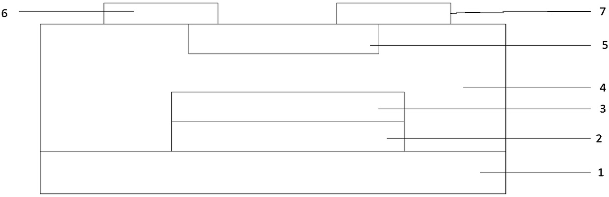
[0042] This embodiment discloses a thin film transistor, which includes a gate, a gate insulating layer, a semiconductor layer, a source and a drain, and also includes a photoelectric conversion layer in contact with the gate, and the photoelectric conversion layer is used for An induced potential is generated in the environment.

[0043] The thin film transistor of the present invention may be a thin film transistor with a top gate structure, or a thin film transistor with a bottom gate structure.

[0044] The thin film transistor of the present invention includes the arrangement of general film layers, such as gate, gate i...


PUM


Abstract

The invention relates to a TFT, a preparation method thereof and a display device, and belongs to the display field. The TFT comprises a photoelectric conversion layer which makes contact with a gateelectrode and is used to generate inductive potential in the illumination environment. The photoelectric conversion layer receives illumination and generates the inductive potential, and the gate electrode can be compensated and carries out voltage driving; and thus, in practical operation, the TFT can be conductive via a lower voltage provided by the external, and an energy-saving effect is substantial. When the TFT is used for the display device, power consumption of the display device can be reduced, and a higher energy efficiency ratio can be realized.

Description

technical field [0001] The invention relates to the display field, in particular to a thin film transistor, a preparation method thereof and a display device. Background technique [0002] A thin film transistor is a field effect semiconductor device, which plays an important role especially in flat panel display devices. The thin film transistor includes several important components such as a substrate, a gate, a gate insulating layer, a semiconductor layer, and source and drain. According to the difference in the relative position of the gate and the semiconductor layer, it can be specifically divided into a thin film transistor with a top gate structure and a thin film transistor with a bottom gate structure. With the development of display technology towards high resolution, large size and high frame rate, there are higher requirements for the driving capability of thin film transistors. [0003] At present, the driving mode of the thin film transistor is to drive the g...

Claims


Application Information

Patent Timeline
Patent Type & Authority Applications(China)
IPC IPC(8): H01L51/42H01L51/48
CPCH10K71/12H10K30/65H10K30/50Y02E10/549H01L29/4908H01L29/7869Y02P70/50H01L29/786H10K30/10H10K30/81H10K10/462
Inventor 刘松温钰孙建明李正亮马啸尘胡合合张文林杜建华宁策
Owner BOE TECH GRP CO LTD