Novel deburring device for ceramic dielectric chip of high-voltage ceramic capacitor

A high-voltage ceramic, burr removal technology, applied in capacitors, capacitor manufacturing, circuits, etc., can solve problems such as increasing the bearing pressure and load of the motor, failing to meet the requirements of the product, reducing the stability of equipment operation, and reducing the load. Pressure and load capacity, simple structure, the effect of improving the service life

Inactive Publication Date: 2018-08-17
SUZHOU HONGQUAN HIGH VOLTAGE CAPACITOR
View PDF5 Cites 7 Cited by
  • Summary
  • Abstract
  • Description
  • Claims
  • Application Information

AI Technical Summary

Problems solved by technology

[0003] However, the existing ceramic dielectric chip burr removal device manually rotates and wipes the corners of the ceramic dielectric chip, which has high labor intensity, low production efficiency, and uneven chamfering, which is prone to pits and missing chamfering. The structure of the deburring device is not stable enough. When deburring the chamfering, it is easy to cause the displacement of the upper and lower mold bases, which reduces the quality of the chamfering. There is also a deburring device that installs the motor at the bottom of the lower mold base to drive the lower mold base. Rotation increases the bearing pressure and load capacity of the motor, reduces the stability of equipment operation, and reduces the service life, which is far from meeting the current people's requirements for this product.

Method used


Image

  • Novel deburring device for ceramic dielectric chip of high-voltage ceramic capacitor
  • Novel deburring device for ceramic dielectric chip of high-voltage ceramic capacitor
  • Novel deburring device for ceramic dielectric chip of high-voltage ceramic capacitor

Examples


Embodiment Construction

[0019] The present invention will be further described below in conjunction with specific embodiments, wherein, the accompanying drawings are only for exemplary illustrations, and what is shown is only a schematic diagram, rather than a physical map, and cannot be understood as a limitation to this patent. In order to better illustrate the present invention Specific embodiments, it is understandable that some well-known structures and their descriptions may be omitted in the drawings. Based on the specific embodiments of the present invention, all other specific implementations obtained by those skilled in the art without creative work way, all belong to the protection scope of the present invention.

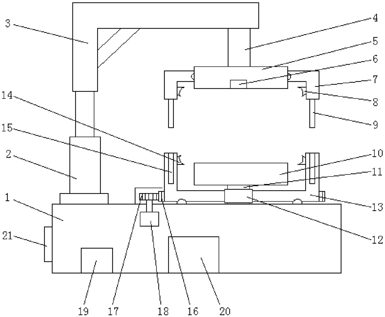
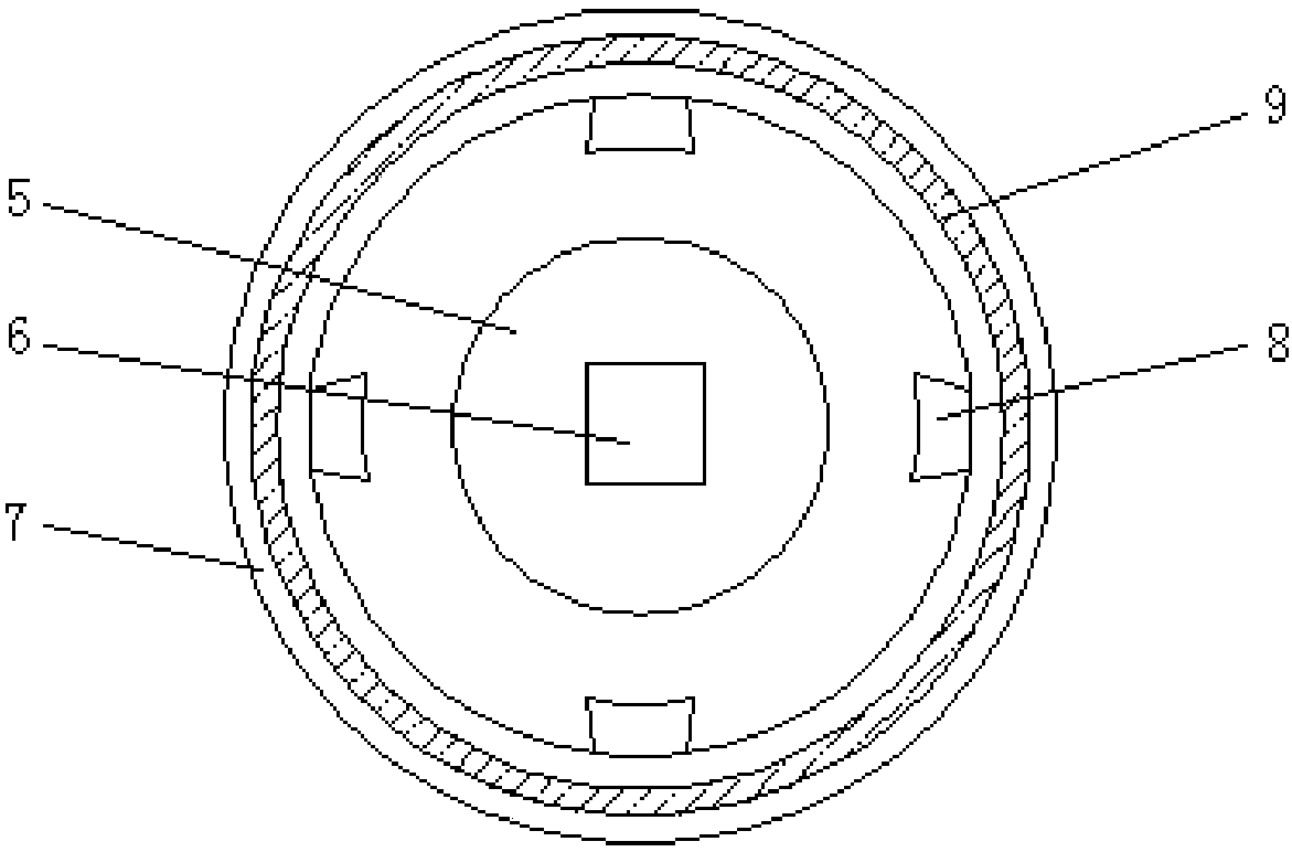
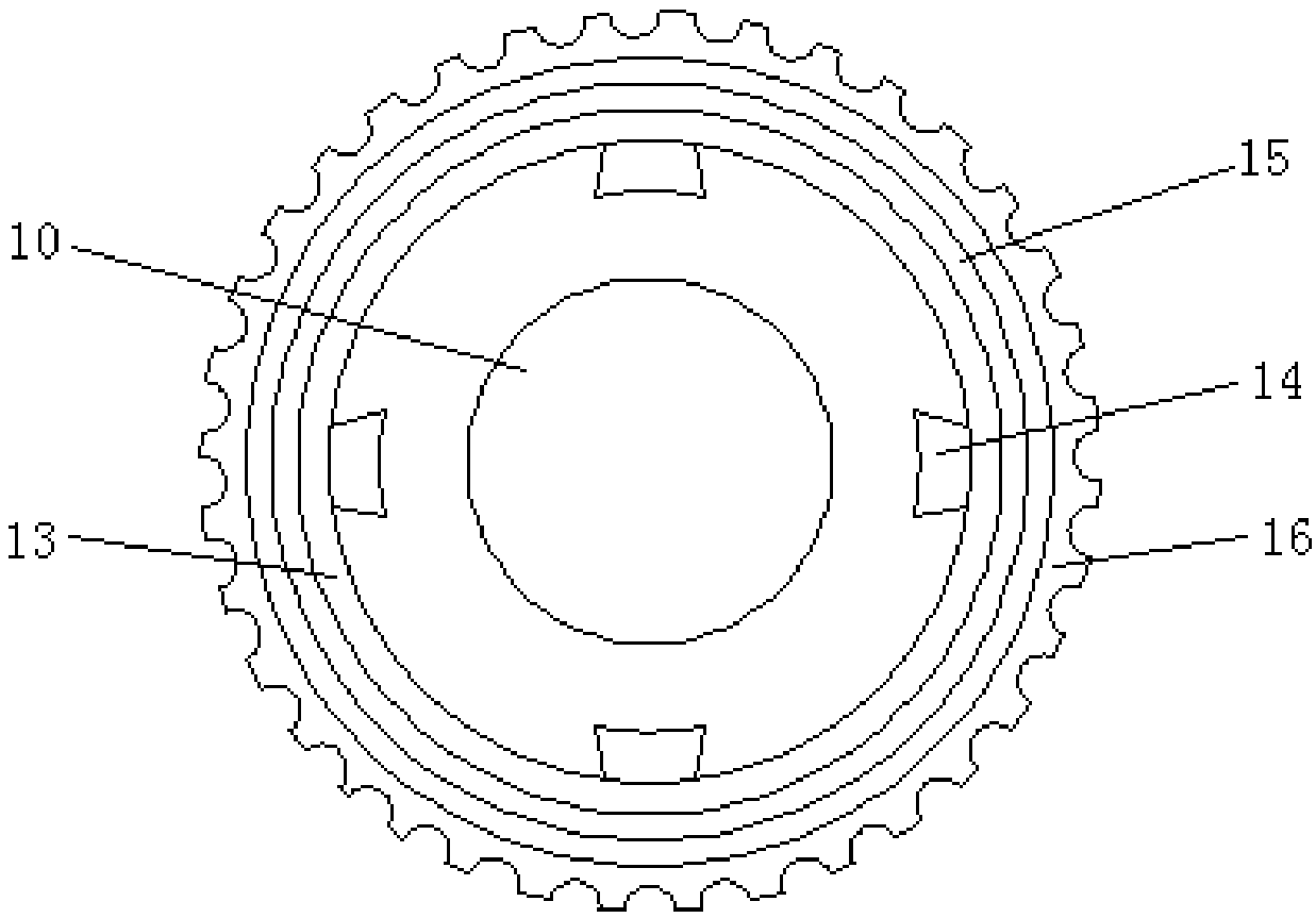
[0020] see Figure 1-Figure 3 , the present invention provides a technical solution: a novel device for removing burrs from ceramic dielectric chips of high-voltage ceramic capacitors, including a workbench 1, a cylinder 2 is vertically connected to the left side of the top of t...


PUM


Abstract

The invention discloses a novel deburring device for the ceramic dielectric chip of a high-voltage ceramic capacitor. The novel deburring device comprises a workbench and is characterized in that an air cylinder is vertically connected to the left side of the top of the workbench, a hanging bracket is connected to the top end of the air cylinder in a threaded and sleeved manner, a vertical upper support column is connected to the right side of the bottom of the hanging bracket, a horizontal lower pressing plate is connected to the bottom of the upper support column, a pressure center is embedded into the center of the bottom of the lower pressing plate, an upper die seat is rotatably connected to the outer side of the lower pressing plate through a slide rail, upper cutters are evenly symmetrically connected to the inner side of the bottom of the upper die seat, and a vertical annular positioning pin is arranged on the outer side of each upper cutter. The novel deburring device is simple in structure, stable and reliable, convenient to mount and demount, simple to operate, capable of simultaneously performing even and thorough chamfering on the top and the bottom of the ceramic dielectric chip, capable of stably fixing the ceramic dielectric chip, capable of preventing the displacement of upper and lower die seats, capable of increasing chamfering quality, capable of reducing motor bearing pressure and load and capable of increasing equipment operation stability.

Description

technical field [0001] The invention relates to the technical field of ceramic capacitor production, in particular to a novel device for removing burrs from ceramic dielectric chips of high-voltage ceramic capacitors. Background technique [0002] Ceramic capacitors are also called ceramic capacitors or monolithic capacitors. As the name implies, ceramic capacitors are capacitors whose dielectric material is ceramic. Mainly, while the ceramic dielectric chip in the ceramic capacitor, in the molding and pressing stage, there will be a sharp part of the chamfer, because the sharp part will cause poor painting of the corners in the subsequent spraying process, resulting in poor voltage resistance. Therefore, in After the molding and pressing are completed, it will be required to chamfer and deburr the corners of the ceramic dielectric chip. [0003] However, the existing ceramic dielectric chip burr removal device manually rotates and wipes the corners of the ceramic dielectri...

Claims


Application Information

Patent Timeline
Patent Type & Authority Applications(China)
IPC IPC(8): H01G13/00
CPCH01G13/00
Inventor 钱云春
Owner SUZHOU HONGQUAN HIGH VOLTAGE CAPACITOR
Why Eureka
Try Eureka