HDR image sensor pixel structure and imaging system supporting multiple exposure modes
An image sensor and pixel structure technology, applied in the field of image sensors, can solve the problem that the pixel structure cannot support multiple exposure modes, etc., and achieve the effect of high dynamic range characteristics
- Summary
- Abstract
- Description
- Claims
- Application Information
AI Technical Summary
Problems solved by technology
Method used
Image
Examples
Embodiment 1
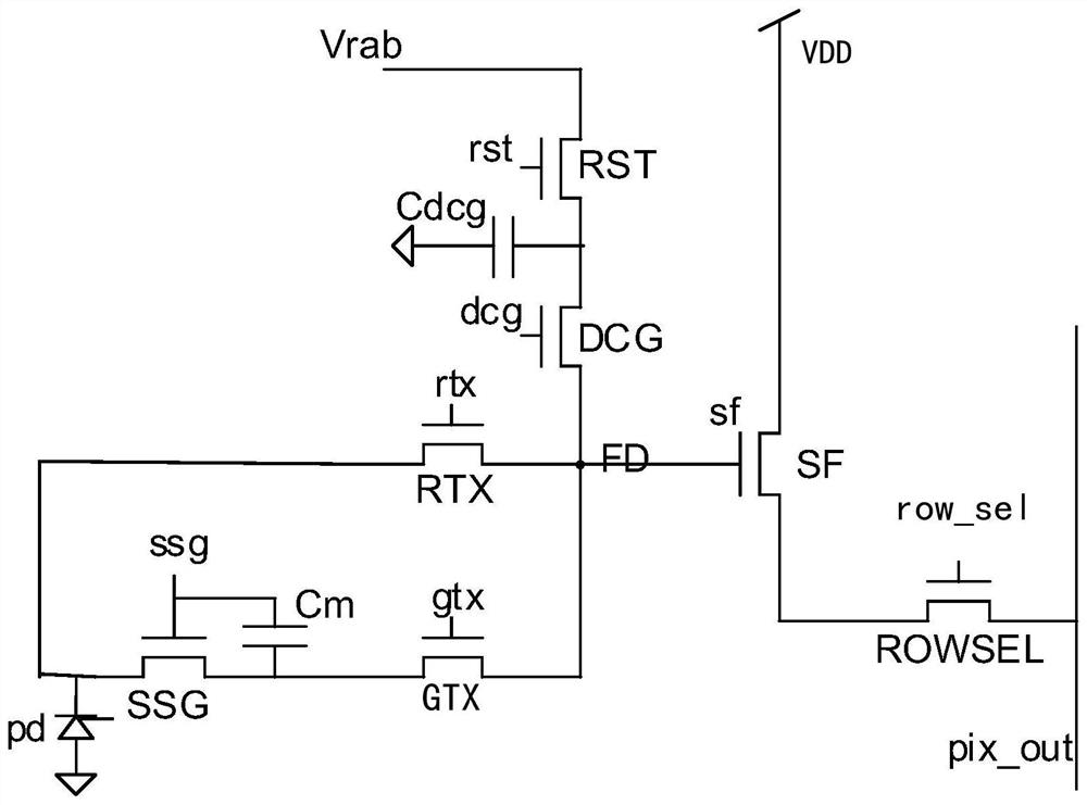
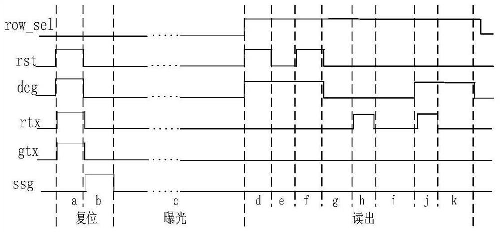
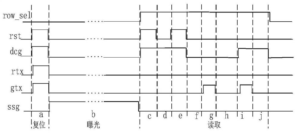
[0072] see figure 1 ,Such as figure 1 As shown, the HDR image sensor pixel structure supporting multiple exposure modes provided by the embodiment of the present invention includes a photodiode pd for accumulating charges generated by the photoelectric effect in response to incident light, the photodiode has a first terminal and a second terminal, The first terminal is connected to the ground terminal, and the second terminal is respectively coupled to the floating diffusion node FD through two branches, one of which is a rolling exposure transmission unit, and the other branch is a global exposure transmission unit; in this embodiment , the rolling exposure transfer unit is a rolling exposure transfer transistor RTX, and the second terminal of the photodiode pd is coupled to the floating diffusion node FD through the rolling exposure transfer transistor RTX. The global exposure transfer unit includes a global exposure transfer transistor GTX, an exposure control transistor S...
Embodiment 2
[0136] see Image 6 ,Such as Image 6 As shown, compared with Embodiment 1, in the HDR image sensor pixel structure supporting multiple exposure modes provided by the embodiment of the present invention, the storage capacitor Cm and the double conversion gain capacitor Cdcg are both parasitic capacitances. Specifically, the storage capacitor Cm is The parasitic capacitance of the exposure control transistor SSG, the dual conversion gain capacitor Cdcg is the parasitic capacitance of the connection point of the reset transistor RST and the dual conversion gain control transistor DCG to ground. Apart from this, other aspects of this embodiment are the same as those of Embodiment 1, and will not be repeated here. Of course, it should be appreciated that it can also be set that the storage capacitor Cm is a parasitic capacitance, and the dual conversion gain capacitor Cdcg is a separate capacitor, or the storage capacitor Cm is a separate capacitor, and the double conversion gain...
Embodiment 3
[0138] see Figure 7 ,Such as Figure 7 As shown, the HDR image sensor pixel structure supporting multiple exposure modes provided by this embodiment includes a photodiode pd, a reset transistor RST, and a dual conversion gain control unit; wherein, the photodiode pd is used to accumulate the charge generated by the photoelectric effect in response to the incident light, the photodiode pd has a first terminal and a second terminal, the first terminal is connected to the ground terminal, and the second terminal is coupled to the floating diffusion node FD through a rolling exposure transfer unit, specifically, the rolling exposure transfer unit is a rolling exposure transfer transistor RTX. A first terminal of the reset transistor RST is coupled to a first voltage source Vrab, and a second terminal thereof is coupled to a floating diffusion node FD through a dual conversion gain control unit; wherein the first voltage source Vrab is an independent voltage source. Specifically...
PUM
 Abstract
Description
Claims
Application Information


