Image sensor pixel structure and imaging system immune to LED light source flicker
An image sensor and LED light source technology, which is applied in the field of image sensors, can solve the problems of not being able to adapt to LED light source flickering, and achieve the effects of avoiding the loss of LED light source information, preventing overexposure, and high dynamic range characteristics
- Summary
- Abstract
- Description
- Claims
- Application Information
AI Technical Summary
Problems solved by technology
Method used
Image
Examples
Embodiment 1
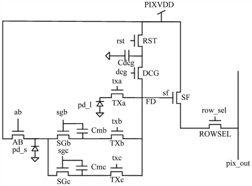
[0063] see figure 1 ,Such as figure 1 As shown, the image sensor pixel structure immune to LED light source flicker provided by the embodiment of the present invention includes a large-area photodiode pd_1 and a small-area photodiode pd_s for accumulating charges generated by the photoelectric effect to respond to incident light, wherein the large-area photodiode pd_s The first terminal of the diode pd_1 is connected to the ground terminal, and the second terminal thereof is coupled to the floating diffusion node FD through the first transfer transistor LTX, wherein the first terminal of the large-area photodiode pd_1 is an anode terminal, and its second terminal is a cathode terminal. The first terminal of the small-area photodiode pd_s is connected to the ground terminal, and the second terminal thereof is coupled to the first voltage source PIXVDD through the first control transistor AB. And the small-area photodiode pd_s is also coupled to the floating diffusion node FD t...
Embodiment 2
[0093] see Figure 4 ,Such as Figure 4 As shown, compared with Embodiment 1, in the image sensor pixel structure immune to LED light source flicker provided by the embodiment of the present invention, the first storage capacitor Cmb, the second storage capacitor Cmc and the double conversion gain capacitor Cdcg are all parasitic capacitances, Specifically, the first storage capacitor Cmb is the parasitic capacitance of the first exposure control transistor SGb, the second storage capacitor Cmb is the parasitic capacitance of the second exposure control transistor SGb, the dual conversion gain capacitor Cdcg is the reset transistor RST and the dual conversion gain control transistor The parasitic capacitance of the connection point of DCG to ground. Apart from this, other aspects of this embodiment are the same as those of Embodiment 1, and will not be repeated here. Of course, it should be appreciated that any one or both of the first storage capacitor Cmb, the second stora...
Embodiment 3
[0095] see Figure 5 ,Such as Figure 5 As shown, this embodiment provides an imaging system 100, including a pixel array 110, the pixel array 110 is arranged in rows and columns, and the structure of each pixel in the pixel array 110 can be the embodiment 1 to embodiment 2 For any one of the pixel structures, please refer to Embodiment 1 to Embodiment 2 for details of the pixel structure, which will not be repeated here.
[0096] In addition, as an exemplary embodiment, the imaging system further includes a logic control unit 120, a drive unit, a column A / D conversion unit 150, and an image processing unit 160; wherein:
[0097] The logic control unit 120 is used to control the working sequence logic of the whole system;
[0098] One end of the drive unit is connected to the logic control unit 120, and the other end is coupled to the pixel array 110 for driving and controlling each control signal line in the pixel array 110; specifically, the drive unit includes a row drive...
PUM
 Abstract
Description
Claims
Application Information


