On-batch silicon wafer lining treatment device in sputtering process
A substrate processing device and sputtering process technology, which is applied in the direction of sputtering plating, metal material coating process, ion implantation plating, etc., can solve the problems of production efficiency reduction, achieve heating uniformity improvement, and avoid efficiency reduction , The effect of improving the treatment effect
- Summary
- Abstract
- Description
- Claims
- Application Information
AI Technical Summary
Problems solved by technology
Method used
Image

Examples
Embodiment 1
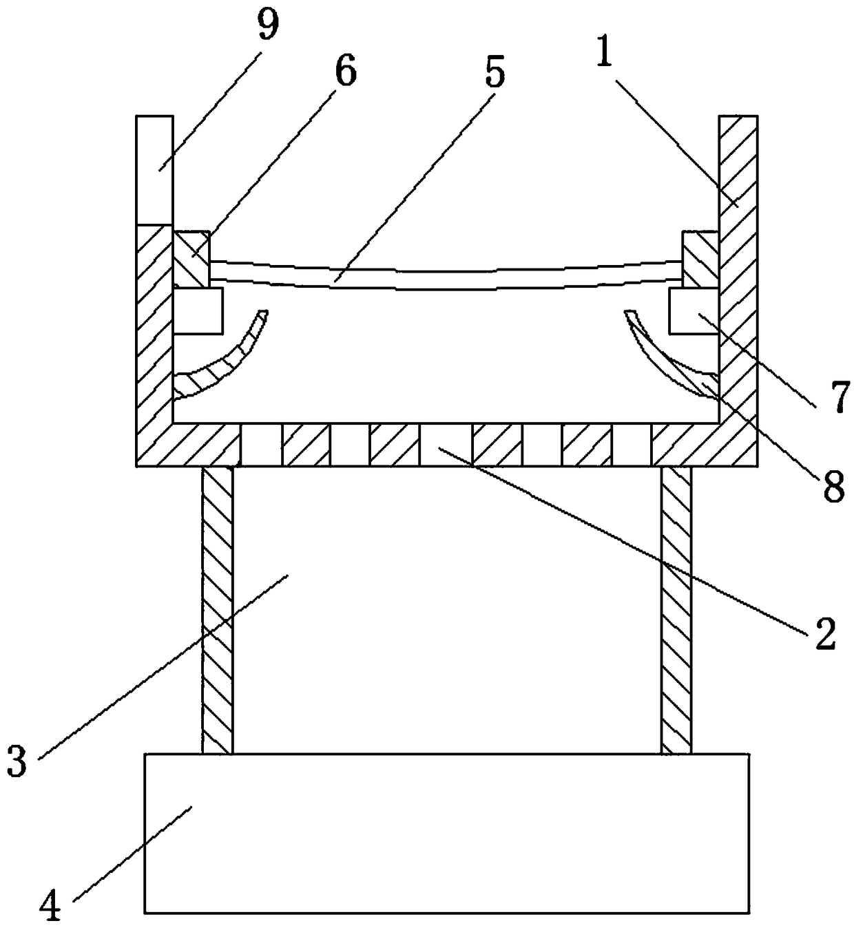
[0015] Such as figure 1 A batch silicon wafer substrate processing device in a sputtering process is shown, which includes a placement tray 1 for placing silicon wafers; the bottom end surface of the placement tray 1 is provided with a plurality of heating holes 2, and the heating holes 2 communicate with each other. To the heating pipeline 3 arranged on the outside of the placement tray 1, the heating pipeline 3 is connected to the heating source 4; the placement tray 1 is provided with a filter screen 5 extending in the horizontal direction, and the edge of the filter screen 5 is provided with a supporting frame 6. The support frame 6 is fixedly arranged on the side end surface of the placement tray 1; in the placement tray 1, the bottom end of the support frame 6 is provided with a plurality of vibration motors 7, and the plurality of vibration motors 7 are aligned with the axis of the support frame 6. rotational symmetry.
[0016] As an improvement of the present inventio...
Embodiment 2
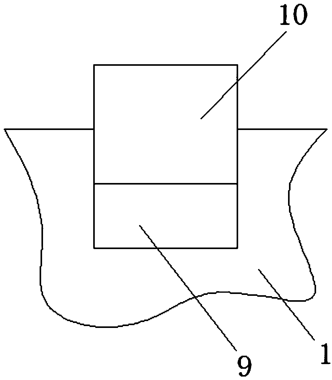
[0020] As an improvement of the present invention, such as figure 2 As shown, the side end surface of the placement tray 1 is provided with a discharge trough 9, and the discharge trough 9 extends between the support frame 6 and the upper end of the placement tray 1; , A discharge baffle 10 is arranged in the discharge chute 9, which extends to the inside of the chute. With the above design, after the substrate processing of the silicon wafers is completed, the silicon wafers processed in batches can be dumped out through the unloading chute, so that the overall processing efficiency can be significantly improved.
[0021] The remaining features and advantages of this embodiment are the same as those of Embodiment 1.
PUM
 Abstract
Description
Claims
Application Information
 - R&D Engineer
- R&D Manager
- IP Professional
- Industry Leading Data Capabilities
- Powerful AI technology
- Patent DNA Extraction
Browse by: Latest US Patents, China's latest patents, Technical Efficacy Thesaurus, Application Domain, Technology Topic.
© 2024 PatSnap. All rights reserved.Legal|Privacy policy|Modern Slavery Act Transparency Statement|Sitemap