

Wafer supporting member
A technology for supporting components and wafers, applied in the manufacture of vehicle components, electrical components, semiconductor/solid-state devices, etc., can solve the problems of hindering heat conduction and increasing the temperature difference of wafers, and achieves improved uniform heating, reduced temperature, and detachment characteristics. excellent results
- Summary
- Abstract
- Description
- Claims
- Application Information
AI Technical Summary
Problems solved by technology
Method used
Image

Examples
no. 1 approach
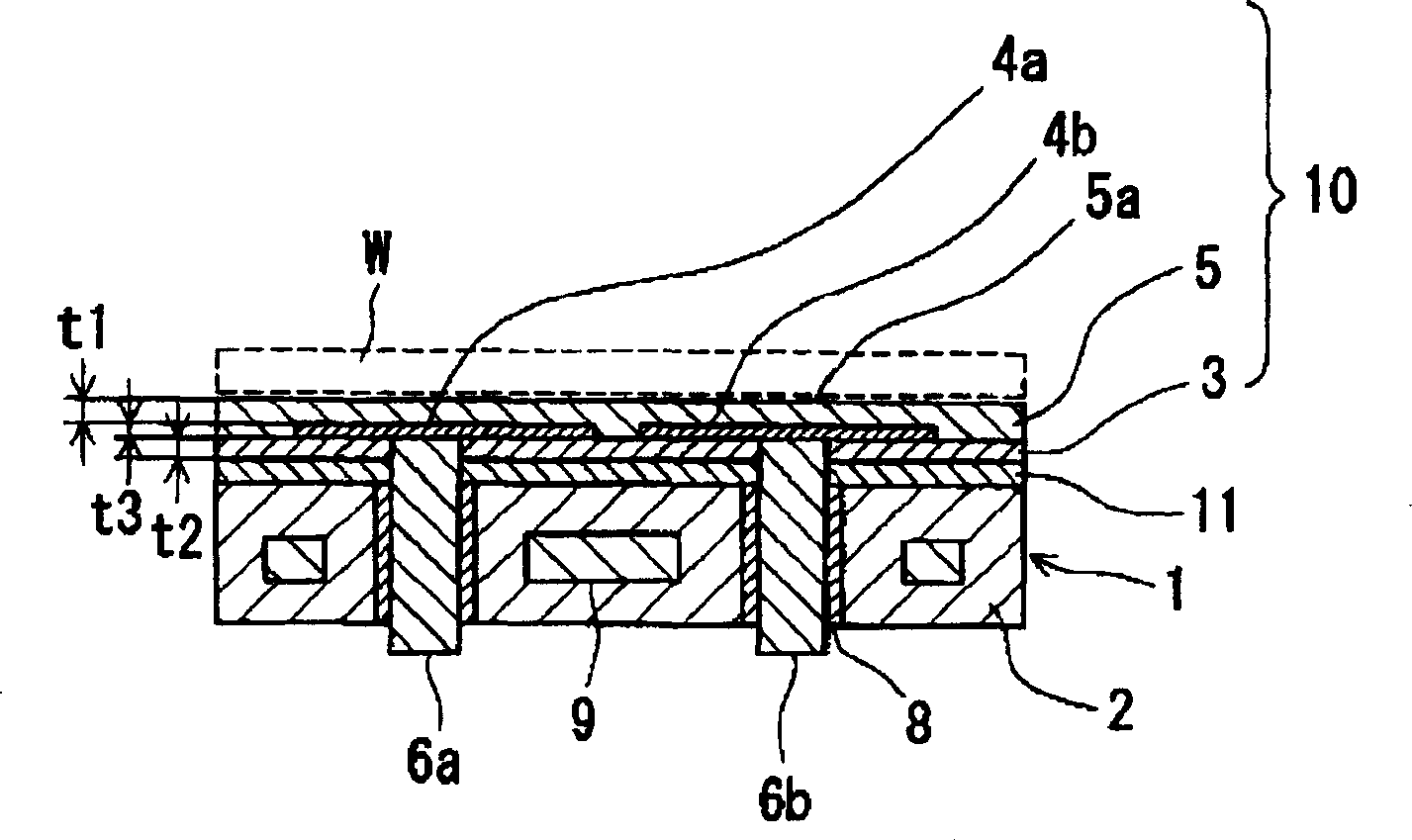
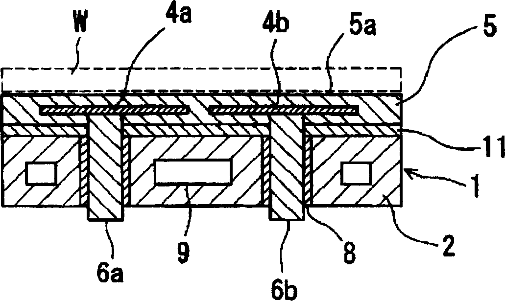
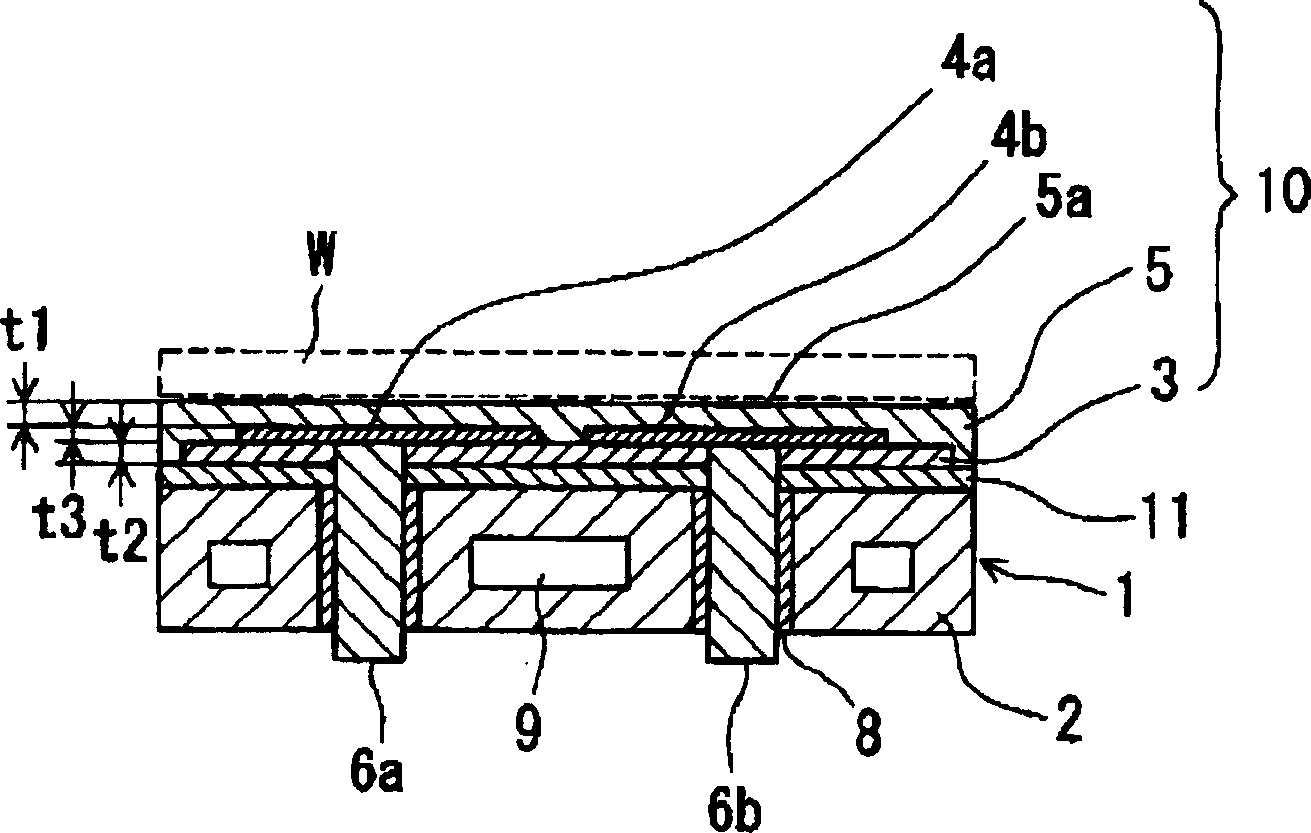
[0056] Hereinafter, the first embodiment (electrostatic chuck) of the present invention will be described in detail.
[0057] In the preferred embodiment of the present invention, it is provided with a support part having a main surface on one side as a loading surface for loading a wafer, and a support portion with an insulating film and an insulating layer for the adsorption electrode built-in on the other main surface, and occasionally built-in bonding The insulating resin layer of the heater on the main surface where the adsorption electrode is installed nearby has a conductive base part through which a cooling medium flows. The volume resistivity of the insulating resin layer is 10 8 ~10 14 Ω·cm, the resistance value between the loading surface and the conductive base part is 10 7 ~10 13 Ω is appropriate. Preferably, the insulating film and the insulating layer are composed of the same plate-shaped ceramic body, and the adsorption electrode is embedded in the plate-shaped cer...
Embodiment 1
[0135] 0.5% by mass of calcium oxide and magnesium oxide were added to the alumina powder according to the weight conversion method, and mixed by a ball mill for 48 hours. After removing impurities from the ball or the wall of the ball mill through the 325 mesh wire, the obtained alumina slurry is dried in a dryer at 120°C for 24 hours. The obtained alumina powder is mixed with an acryl-based binder and a solvent to make an alumina slurry. A green tape (Green Tape) was made from the above alumina slurry by the doctor blade method.
[0136] Furthermore, the above-mentioned green tape was fabricated into a laminated body in which several sheets were laminated, and an adsorption electrode made of tungsten carbide paste was printed on one main surface. In addition, a laminate in which several sheets of ceramic printed circuit boards were laminated, and pressurized and compressed to form a laminate.
[0137] In addition, in a nitrogen state, sintered in a sintering furnace consisting o...
Embodiment 2
[0158] In the same manner as in Example 1, a supporting member such as a wafer composed of aluminum oxide and aluminum nitride was produced. Aluminum nitride uses a method of changing the addition amount of cerium oxide within the range of 1 to 15% by mass to change the volume resistivity of the material. In addition, the resin layer produced a sample whose volume resistivity was changed by changing the content of Al. Also, the same evaluation as in Example 1 was made. Then, the electrical impedance between the mounting surface of each sample and the conductive base part was measured.
[0159] Moreover, the impedance between the mounting surface and the conductive base part is that an electrode with a diameter of 10 mm is provided on the mounting surface to detect the electrical resistance value between the electrode and the conductive base part. Then, it is converted into the area of the mounting surface and set as the resistance value between the mounting surface and the condu...
PUM
 Abstract
Description
Claims
Application Information