Ceramic double-side three-dimensional integrated structure and packaging method of ultra-wideband radio frequency micro-system

A three-dimensional integration and micro-system technology, applied in the direction of electrical components, electrical solid devices, circuits, etc., can solve the problems of difficulty in adapting to the development needs of micro-system integration of electronic equipment, limited integration density, and interconnection interface occupancy, etc., to achieve internal integration density The effect of lifting, fewer assembly steps, and lower volume occupancy

Active Publication Date: 2018-08-21
SOUTHWEST CHINA RES INST OF ELECTRONICS EQUIP
View PDF8 Cites 21 Cited by
  • Summary
  • Abstract
  • Description
  • Claims
  • Application Information

AI Technical Summary

Problems solved by technology

Most of the existing RF packages based on multilayer ceramic substrates are single-sided integration. Even if organic substrates are used for double-sided integration, metal casings are required for airtightness. There is a limited integration density, and hermetic packaging and interconnection ports will occupy a large area. The volume problem makes it difficult to adapt to the development needs of electronic equipment microsystem integration

Method used


Image

  • Ceramic double-side three-dimensional integrated structure and packaging method of ultra-wideband radio frequency micro-system
  • Ceramic double-side three-dimensional integrated structure and packaging method of ultra-wideband radio frequency micro-system
  • Ceramic double-side three-dimensional integrated structure and packaging method of ultra-wideband radio frequency micro-system

Examples


example 1

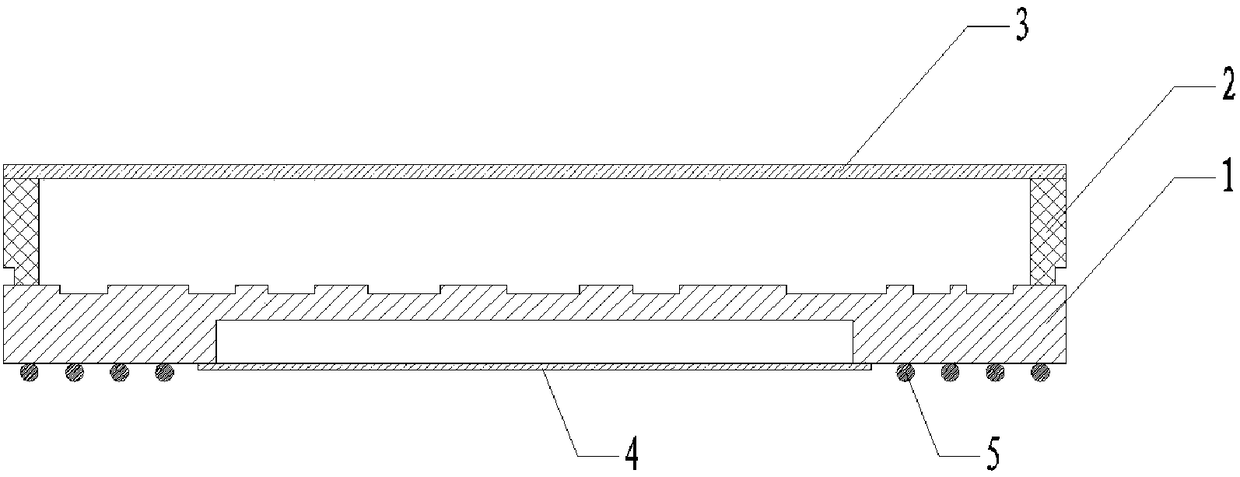
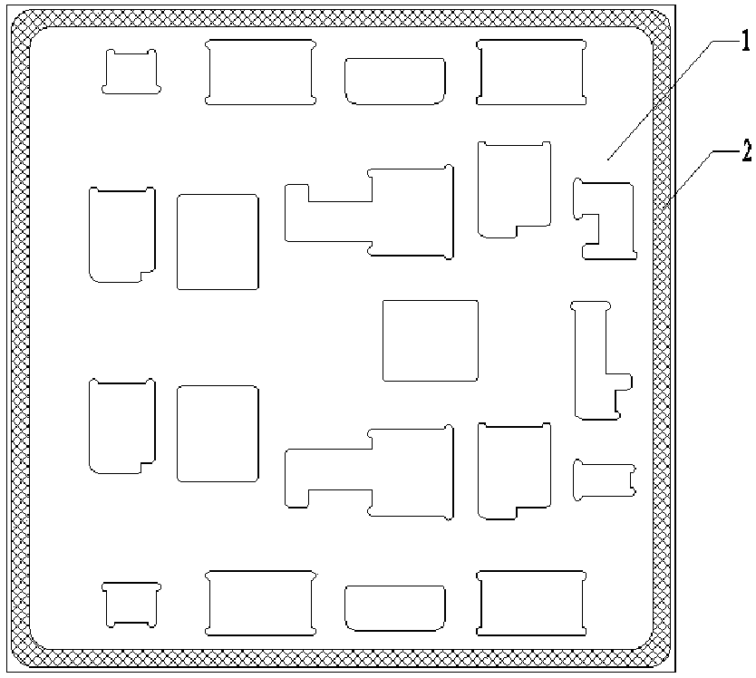
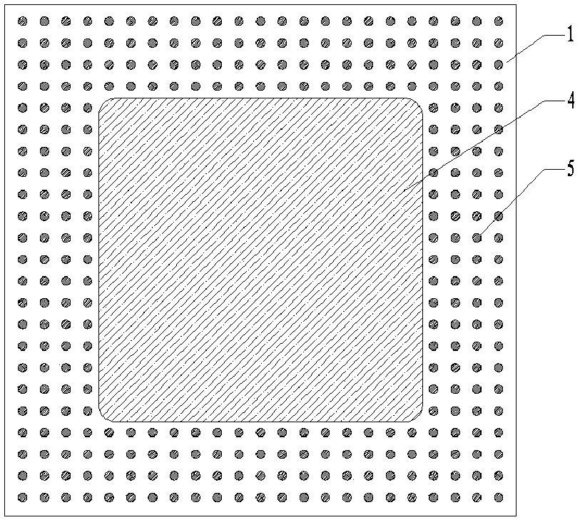
[0045] The multilayer ceramic double-sided three-dimensional integrated architecture of this example ultra-wideband RF microsystem is as follows: figure 1 , figure 2 and image 3 shown. Including multilayer ceramic substrate 1, metal micro frame 2, front cover 3, back cover 4 and BGA solder balls 5:

[0046] Both sides of the multilayer ceramic substrate 1 are provided with cavities for installing chips, the metal micro frame 2 is welded on the front of the multilayer ceramic substrate 1, and the front cover plate 3 is welded on the metal micro frame 2, The back cover plate 4 is welded on the back cavity groove of the multilayer ceramic substrate 1, BGA pads are arranged on the back side of the multilayer ceramic substrate 1 except the back cover plate 4, and the BGA solder balls 5 pass through the BGA pads Soldered on the back of the multilayer ceramic substrate 1.

[0047] The packaging method of the multilayer ceramic double-sided three-dimensional integrated architect...


PUM


Abstract

The invention provides a ceramic double-sided three-dimensional integrated structure of an ultra-wideband radio frequency micro-system and belongs to the technical field of ultra-wideband radio frequency packaging. The structure comprises a ceramic substrate, a metal micro frame, a front cover plate, a back cover plate and a BGA solder ball. Both sides of the ceramic substrate are provided with cavity grooves for mounting chips. The metal micro frame is welded on the front surface of the ceramic substrate. The front cover plate is welded on the metal micro frame. The back cover plate is weldedon the back cavity groove of the ceramic substrate. The back surface of the ceramic substrate except the back cover plate is provided with a BGA solder pad. The BGA solder ball is welded on the backsurface of the ceramic substrate through the BGA solder pad. The invention also provides a packaging method of the integrated structure. According to the invention, the internal integration density nearly is doubled. The volume occupancy rate of external interconnection interface and airtight package is greatly reduced. The structure has the advantages of simple structure and less procedure and isan effective method for realizing the three-dimensional stacking of the ultra-wideband radio frequency micro-system.

Description

technical field [0001] The invention belongs to the technical field of ultra-wideband radio frequency packaging, and specifically relates to a ceramic double-sided three-dimensional integrated structure and a packaging method of an ultra-wideband radio frequency microsystem. Background technique [0002] With the urgent need for miniaturization of military electronic equipment, broadband radio frequency packaging is developing towards higher density, higher frequency, and smaller interconnection interfaces. Most of the existing RF packages based on multilayer ceramic substrates are integrated on one side. Even if organic substrates are used for double-sided integration, metal shells need to be used for airtightness. There is a limited integration density, and hermetic packaging and interconnection ports will occupy a large area. Due to the volume problem, it is difficult to adapt to the development needs of electronic equipment microsystem integration. Contents of the inve...

Claims


Application Information

Patent Timeline
Patent Type & Authority Applications(China)
IPC IPC(8): H01L23/13H01L23/488H01L21/50H01L21/56
CPCH01L21/50H01L21/56H01L23/13H01L23/488
Inventor 张继帆张正鸿董东肖庆
Owner SOUTHWEST CHINA RES INST OF ELECTRONICS EQUIP
Why Eureka
Try Eureka