Semiconductor device with interdigitated electrodes

A semiconductor and interdigitated technology, which is applied in the field of semiconductor devices with interdigitated electrodes, can solve problems such as the existence of high electric fields, the inability to extend high electric fields, and high on-resistance, and achieve the effect of chip scale control and good chip scale

Active Publication Date: 2018-08-21
苏州量芯微半导体有限公司
View PDF11 Cites 1 Cited by
  • Summary
  • Abstract
  • Description
  • Claims
  • Application Information

AI Technical Summary

Problems solved by technology

However, we will show that there are limitations to this design, such as the presence of high electric fields at the corners that cannot extend to other parts of the fingers
In addition, due to uneven current or electric field distribution, the existing electrode layout designs basically have potential defects of high on-resistance or low breakdown voltage.

Method used


Image

  • Semiconductor device with interdigitated electrodes
  • Semiconductor device with interdigitated electrodes
  • Semiconductor device with interdigitated electrodes

Examples


Embodiment Construction

[0032] The specific embodiments of the present invention will be described in detail below in conjunction with the accompanying drawings, but it should be understood that the protection scope of the present invention is not limited by the specific embodiments.

[0033] Unless expressly stated otherwise, throughout the specification and claims, the term "comprise" or variations thereof such as "includes" or "includes" and the like will be understood to include the stated elements or constituents, and not Other elements or other components are not excluded.

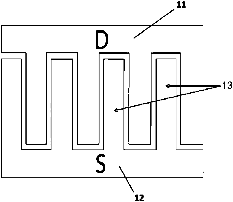
[0034] figure 1 It is a schematic diagram of an interdigitated electrode in the prior art. The semiconductor device includes a drain (D), a source (S), a drain electrode base 11 and a source electrode base 12, and interdigitated electrodes are arranged between the drain and the source. It can be seen from the figure that the interdigitated electrodes in the prior art are all regular rectangular interdigitated fingers, and...


PUM


Abstract

Disclosed is a semiconductor device with interdigitated electrodes. The semiconductor device includes a drain electrode, a source electrode, and a plurality of interdigital electrodes, and each of theinterdigital electrodes is provided with two crossed interdigital fingers respectively connected to a drain-electrode substrate and a source-electrode substrate, at least one semiconductor conductingarea is arranged between any two interdigital electrodes among the interdigital electrodes, wherein the interdigital fingers are in an asymmetric shape, and the fingertips of the interdigital fingersare in a non-linear shape. By the adoption of the interdigital electrodes, the current or power can be uniformly distributed on the surface of the whole chip. The interdigital electrodes provided bythe invention are provided with electrode substrates with a variable width, so that the flow distribution on the metal can be effectively controlled and the scale of the chip can be well controlled.

Description

technical field [0001] The invention relates to a semiconductor device, in particular to a semiconductor device with interdigitated electrodes. Background technique [0002] In recent years, with the development of semiconductor technology, third-generation semiconductor materials such as GaN, AlGaN and other new materials have gradually attracted widespread attention. Since these new semiconductor materials have a wide band gap and are able to form a two-dimensional electron gas (2DEG) at the AlGaN / GaN heterojunction interface, they have been widely used to fabricate high electron mobility transistors (HEMTs), which are extremely The conversion and conduction efficiency of the device are greatly improved. These devices are typically lateral devices, where current can flow close to the surface. [0003] In order to realize various power electronic applications, semiconductor devices are generally required to be able to achieve a current input of 1 to 100 amperes. In later...

Claims


Application Information

Patent Timeline
Patent Type & Authority Applications(China)
IPC IPC(8): H01L29/41H01L29/778
CPCH01L29/41H01L29/778H01L29/401H01L31/1085H01L33/20H01L31/022408H01L33/38H01L29/41758H01L29/7786
Inventor 李湛明傅玥吴卫东刘雁飞
Owner 苏州量芯微半导体有限公司
Why Eureka
Try Eureka