Substrate-to-substrate broadband interconnection structure

A technology for interconnecting structures and substrates, applied in electrical components, connecting devices, circuits, etc., can solve problems such as leakage, difficulty in implementation, and inability to place components, achieve simple process methods, expand working bandwidth, and break the limit of open line width. Effect

Inactive Publication Date: 2018-08-21
NANJING UNIV OF POSTS & TELECOMM +1
View PDF1 Cites 0 Cited by
  • Summary
  • Abstract
  • Description
  • Claims
  • Application Information

AI Technical Summary

Problems solved by technology

[0002] The interconnection structure is used in monolithic microwave integrated circuits and multi-chip modules to realize signal transmission between substrates of different heights, such as Image 6 As shown, one substrate is superimposed on another substrate, and then the interconnection between the substrates is realized through the connection of gold wire bonding wires, but the traditional interconnection between substrates has the following problems: First, the use of multiple gold wire bonding wires And the compensation microstrip open line can effectively increase the bandwidth of the interconnect structure, but the frequency cannot exceed 20 GHz; second, the minimum width required for the compensation open line used to widen the bandwidth of the gold wire bonding interconnect structure is less than 0

Method used


Image

  • Substrate-to-substrate broadband interconnection structure
  • Substrate-to-substrate broadband interconnection structure
  • Substrate-to-substrate broadband interconnection structure

Examples


Example Embodiment

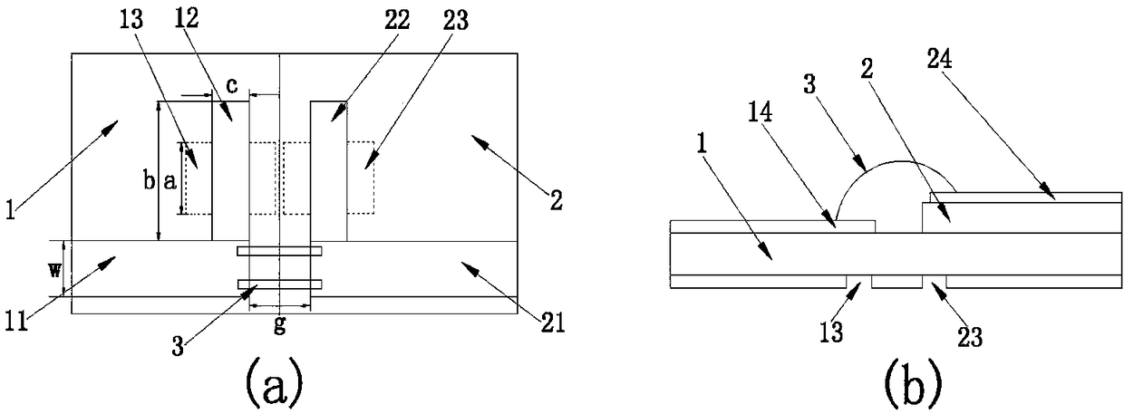
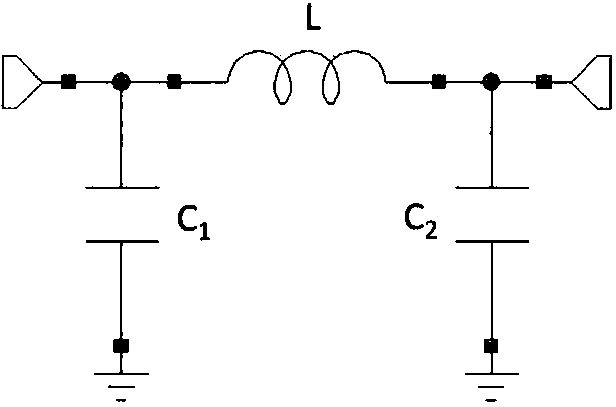
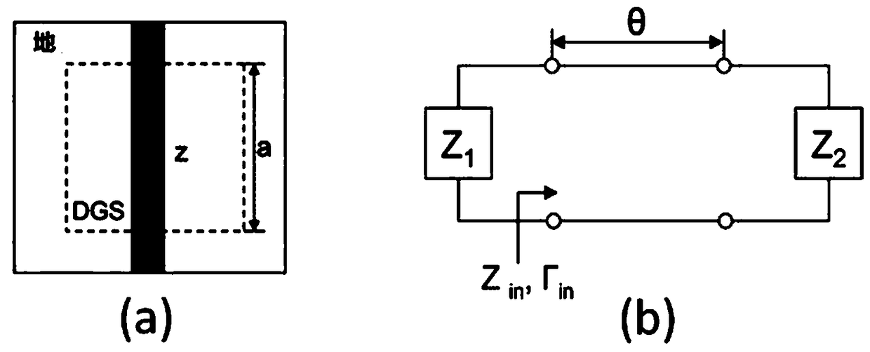
[0018] In order to enable those skilled in the art to better understand the solutions of the present invention, the technical solutions in the embodiments of the present invention will be described clearly and completely in conjunction with the accompanying drawings in the embodiments of the present invention. Obviously, the described embodiments are only a part of the embodiments of the present invention, rather than all the embodiments, and the preferred embodiments of the present invention are shown in the accompanying drawings. The present invention can be implemented in many different forms and is not limited to the embodiments described herein. On the contrary, the purpose of providing these embodiments is to make the understanding of the disclosure of the present invention more thorough and comprehensive. Based on the embodiments of the present invention, all other embodiments obtained by those of ordinary skill in the art without creative work shall fall within the prote...


PUM


Abstract

The invention discloses a substrate-to-substrate broadband interconnection structure. The broadband interconnection structure comprises a first substrate and a second substrate arranged on one side ofthe first substrate, the first substrate is provided with a first microstrip line and a first port, the second substrate is provided with a second microstrip line and a second port, the first port and the second port are connected through a gold wire bonding wire, the broadband interconnection structure further comprises a first open-circuit line arranged on the first substrate and a second open-circuit line arranged on the second substrate, the first open-circuit line is connected with the first port, and the second open-circuit line is connected with the second port; a first defect ground structure is arranged at the corresponding position on the first substrate under the first open-circuit line and used for improving the characteristic impedance of the first microstrip line; a second defect ground structure is arranged at the corresponding position on the first substrate under the second open-circuit line and used for improving the characteristic impedance of the second microstripline, and the first defect ground structure and the second defect ground structure are not communicated. According to the broadband interconnection structure, the overall structure is simple, and thecharacteristic impedance of the microstrip lines is improved.

Description

technical field [0001] The invention relates to the field of electronic structure design, in particular to a substrate-to-substrate broadband interconnection structure. Background technique [0002] The interconnection structure is used in monolithic microwave integrated circuits and multi-chip modules to realize signal transmission between substrates of different heights, such as Figure 6 As shown, one substrate is superimposed on another substrate, and then the interconnection between the substrates is realized through the connection of gold wire bonding wires, but the traditional interconnection between substrates has the following problems: First, the use of multiple gold wire bonding wires And the compensation microstrip open line can effectively increase the bandwidth of the interconnect structure, but the frequency cannot exceed 20 GHz; second, the minimum width required for the compensation open line used to widen the bandwidth of the gold wire bonding interconnect s...

Claims


Application Information

Patent Timeline
IPC IPC(8): H01P5/12
CPCH01P5/12
Inventor 李修贤王柠琳黄龄萱周波
Owner NANJING UNIV OF POSTS & TELECOMM
Why Eureka
Try Eureka