Micro-grain light emitting diode display panel

A technology of light-emitting diodes and display panels, applied to static indicators, identification devices, instruments, etc., can solve the problems of loss of light energy, display devices are difficult to be thin and flexible, and increase the power consumption of liquid crystal display devices, etc., to achieve increased The effect of power consumption

Active Publication Date: 2018-08-24
WUHAN CHINA STAR OPTOELECTRONICS TECH CO LTD
View PDF7 Cites 4 Cited by
  • Summary
  • Abstract
  • Description
  • Claims
  • Application Information

AI Technical Summary

Problems solved by technology

However, the existing liquid crystal display device includes a backlight module, a lower polarizer, an array substrate, a liquid crystal layer, a color filter substrate and an upper polarizer. These laminated structures limit the thickness and shape of the existing liquid crystal display device, resulting in the existing It is difficult for liquid crystal display devices to be thinner and more flexible
In addition, the use of the color filter substrate consumes at least 60% of the light energy, and can only rely on increasing the backlight brightness of the liquid crystal display device to meet the brightness requirements of the actual device, which undoubtedly increases the power consumption of the liquid crystal display device

Method used


Image

  • Micro-grain light emitting diode display panel
  • Micro-grain light emitting diode display panel
  • Micro-grain light emitting diode display panel

Examples


Embodiment Construction

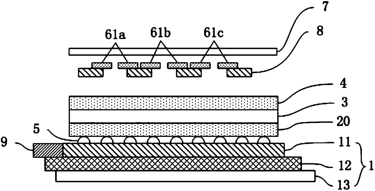
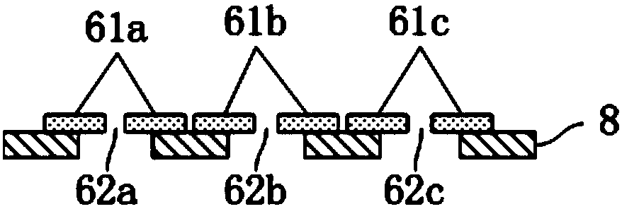
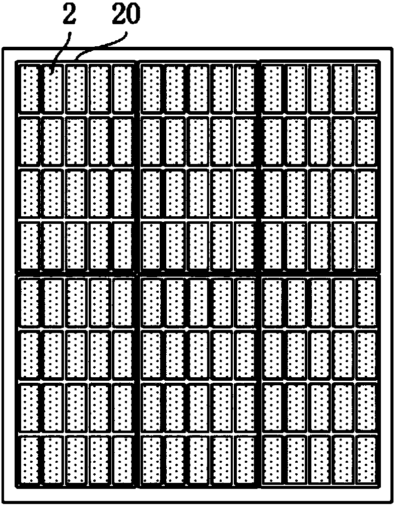
[0027] The present invention provides a microcrystalline light-emitting diode 2 display panel, such as figure 1 As shown, the display panel includes a flexible substrate 1, a plurality of light emitting diodes 2 arranged in an array, a diffraction grating 3 located above the plurality of light emitting diodes 2, a light scattering film 4, and a plurality of light valves located above the light scattering film 4, figure 1 61a, 61b, 61c shown in are light valves. Such as figure 2 As shown, the corresponding openings of the light valves 61a, 61b, and 61c are respectively 62a, 62b, and 62c.

[0028] Wherein, the flexible substrate 1 includes a driving circuit 11, and a plurality of light emitting diodes 2 are fixed on the flexible substrate 1 by flip-chip; white light.

[0029] The diffraction grating 3 is used to split the white light emitted by the light emitting diode 2 to form multiple outgoing lights with different wavelengths.

[0030] The light scattering film 4 is use...


PUM


Abstract

The invention provides a micro-grain light emitting diode display panel, wherein the display panel comprises a flexible substrate, a plurality of light emitting diodes which are distributed in an array form, a diffraction grating and a light scattering film which are arranged at the upper sides of the plurality of light emitting diodes, and a plurality of light valves which are arranged at the upper side of the light scattering film, wherein the flexible substrate comprises a drive circuit, and the plurality of light emitting diodes are fixed to the flexible substrate; the drive circuit is connected to the plurality of light emitting diodes and is used for driving the light emitting diodes to emit white light; the diffraction grating is used for splitting the white light which is emitted by the light emitting diodes, so that various emergent lights which are different in wavelength can be formed; the light scattering film is used for gathering the emergent lights which are same in wavelength and for scattering the emergent lights which are different in wavelength, so that primary light in at least one color is formed; and the plurality of light valves are used for regulating intensity of the primary light. The display panel provided by the invention can become lighter and thinner and can guarantee flexibility, without increase in power consumption of the display panel.

Description

technical field [0001] The invention relates to the field of display technology, in particular to a microcrystalline light-emitting diode display panel. Background technique [0002] At present, light and thin, convenient, energy-saving, delicate picture, cost reduction, and diversified functions are always the development goals of display devices. Meanwhile, as efforts are made to provide various forms of electronic devices, research and development have been conducted to provide various forms of display devices included in the electronic devices. However, the existing liquid crystal display device includes a backlight module, a lower polarizer, an array substrate, a liquid crystal layer, a color filter substrate and an upper polarizer. These laminated structures limit the thickness and shape of the existing liquid crystal display device, resulting in the existing It is difficult for liquid crystal display devices to be thinner and more flexible. In addition, the use of c...

Claims


Application Information

Patent Timeline
Patent Type & Authority Applications(China)
IPC IPC(8): G09F9/33G09F9/30G09G3/32H01L25/18
CPCH01L25/18G09F9/301G09F9/33G09G3/32H01L25/0753H01L33/44H01L25/167
Inventor 程艳
Owner WUHAN CHINA STAR OPTOELECTRONICS TECH CO LTD
Why Eureka
Try Eureka