Millimeter wave frequency multiplier circuit based on relationship between active millimeter wave frequency multiplier base bias voltage and fundamental wave input signal power amplitude

A technology of input signal and base bias, applied in the direction of power oscillators, electrical components, etc., can solve the problem of small harmonic output signal power and frequency conversion gain, so as to improve frequency conversion gain, improve harmonic output signal power, and improve The effect of conversion efficiency

Active Publication Date: 2019-11-01
SOUTHEAST UNIV
View PDF2 Cites 4 Cited by
  • Summary
  • Abstract
  • Description
  • Claims
  • Application Information

AI Technical Summary

Problems solved by technology

[0006] Purpose of the invention: Aiming at the problem that the harmonic output signal power and frequency conversion gain of the existing active millimeter wave frequency multiplier are small, the present invention proposes an active millimeter wave frequency multiplier based on Millimeter-wave frequency multiplier circuit based on the relationship between the base bias voltage of the wave frequency multiplier and the power amplitude of the fundamental wave input signal

Method used


Image

  • Millimeter wave frequency multiplier circuit based on relationship between active millimeter wave frequency multiplier base bias voltage and fundamental wave input signal power amplitude
  • Millimeter wave frequency multiplier circuit based on relationship between active millimeter wave frequency multiplier base bias voltage and fundamental wave input signal power amplitude
  • Millimeter wave frequency multiplier circuit based on relationship between active millimeter wave frequency multiplier base bias voltage and fundamental wave input signal power amplitude

Examples


Embodiment 1

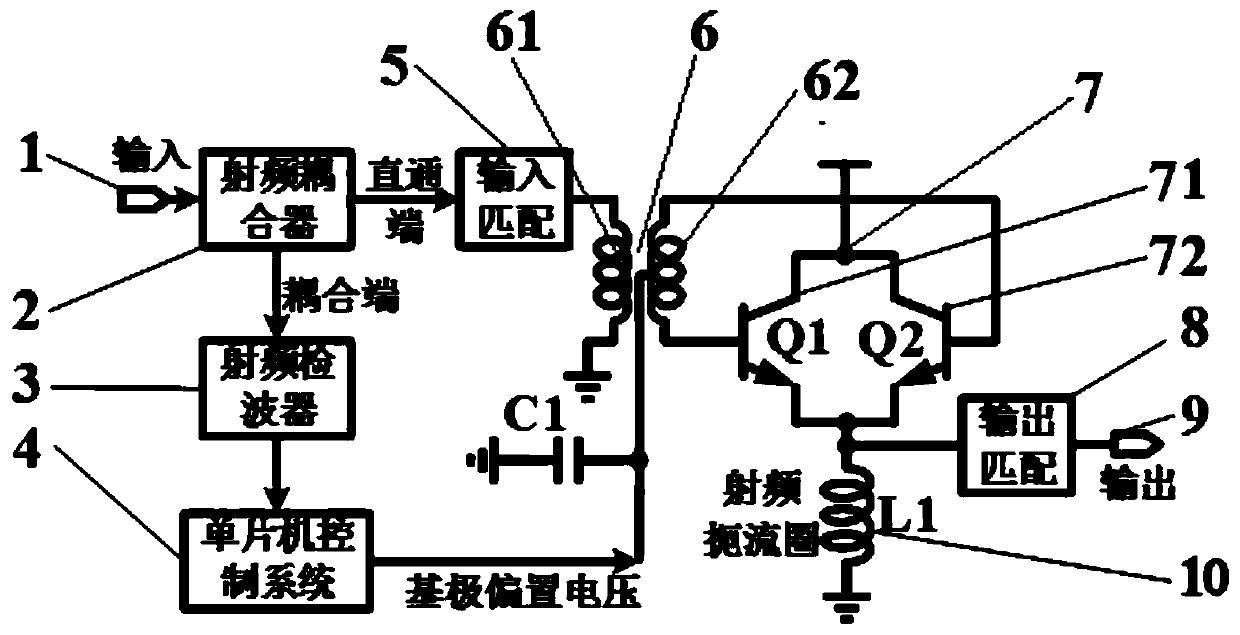
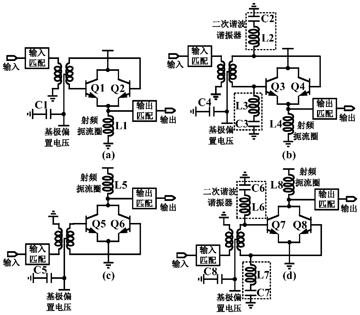
[0026] refer to figure 1 , this embodiment provides a millimeter-wave frequency multiplier circuit based on the relationship between the base bias voltage of the active millimeter-wave frequency multiplier and the power amplitude of the fundamental wave input signal, and the millimeter-wave frequency multiplier system uses a silicon-based bipolar type metal oxide semiconductor integrated circuit technology. Likewise, the millimeter wave can be produced in other ways, and there is no specific requirement, and the process in this embodiment is just one of them.

[0027] The millimeter wave frequency multiplier system includes a fundamental wave signal input terminal 1, a radio frequency coupler 2, a radio frequency detector 3, a single-chip microcomputer control system 4, an input matching 5, a millimeter wave transformer 6, a frequency multiplier core 7, an output matching 8, a harmonic Wave signal output terminal 9 and RF choke coil L110. The fundamental wave signal input te...


PUM


Abstract

The invention discloses a millimeter wave frequency multiplier circuit based on a relationship between active millimeter wave frequency multiplier base bias voltage and fundamental wave input signal power amplitude. A fundamental wave signal input end is connected with a radio frequency coupler, a straight-through end of the radio frequency coupler is connected with input matching, and a couplingend is connected with a radio frequency detector. One end of a primary coil of the millimeter-wave transformer is connected with an input matching output end, and the other end is grounded. The outputend of the radio frequency detector is connected with the input end of the single-chip microcomputer control system. The output end of the single-chip microcomputer control system is connected with aradio frequency center virtual ground point of a secondary coil of the millimeter wave transformer. The two ends of the secondary coil are connected with the two base electrode ends of the frequencymultiplication core respectively, the two emitting electrodes of the frequency multiplication core are connected with the output matching input end, and the output matching output end is connected with the harmonic signal output end. The harmonic output signal power of the active millimeter wave frequency multiplier can be improved, the conversion efficiency from direct current to radio frequencysignals can also be improved, and meanwhile, the power consumption of the active millimeter wave frequency multiplier cannot be increased.

Description

technical field [0001] The present invention relates to the technical field of active millimeter-wave frequency multipliers, in particular to a millimeter-wave frequency multiplier circuit based on the relationship between the base bias voltage of the active millimeter-wave frequency multiplier and the power amplitude of the fundamental wave input signal. Background technique [0002] With the further development of radio technology, the spectrum resources in the low-frequency band are already very crowded. For the needs of future ultra-high-speed communication applications, the channel capacity of the low-frequency band has been difficult to meet the demand. However, in the millimeter wave frequency band, there are still a large number of spectrum resources that have not been developed and utilized. The millimeter wave frequency band is wider and can be used to transmit higher rates, thereby obtaining greater communication capacity. At present, more and more applications fo...

Claims


Application Information

Patent Timeline
Patent Type & Authority Applications(China)
IPC IPC(8): H03B19/14
CPCH03B19/14
Inventor 陈继新周培根严蘋蘋侯德彬洪伟
Owner SOUTHEAST UNIV
Why Eureka
Try Eureka