LED wafer bonding method

A wafer and bonding technology, applied in the direction of semiconductor devices, electrical components, circuits, etc., can solve the problems of low utilization rate of the backplane and occupying precious space of the backplane, and achieve the effect of saving space and improving utilization rate.

Active Publication Date: 2018-08-24
GOERTEK INC
View PDF3 Cites 3 Cited by
  • Summary
  • Abstract
  • Description
  • Claims
  • Application Information

AI Technical Summary

Problems solved by technology

However, with this approach, the alignment marks take up valuable space on the backplane, resulting in poor utilization of the backplane

Method used


Image

  • LED wafer bonding method
  • LED wafer bonding method
  • LED wafer bonding method

Examples


Embodiment Construction

[0035] The preferred embodiments of the present invention will be described below in conjunction with the accompanying drawings. It should be understood that the preferred embodiments described here are only used to illustrate and explain the present invention, and are not intended to limit the present invention, and in the absence of conflict, the present invention The embodiments and the features in the embodiments can be combined with each other.

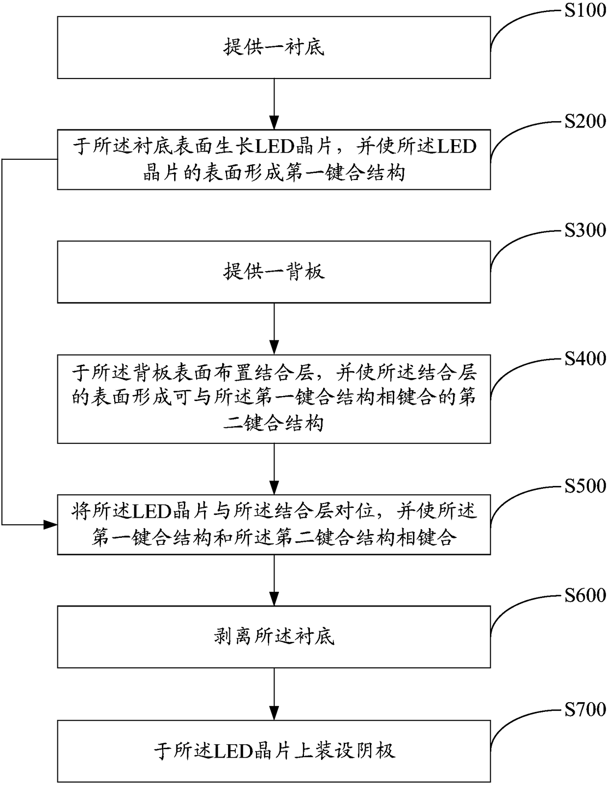
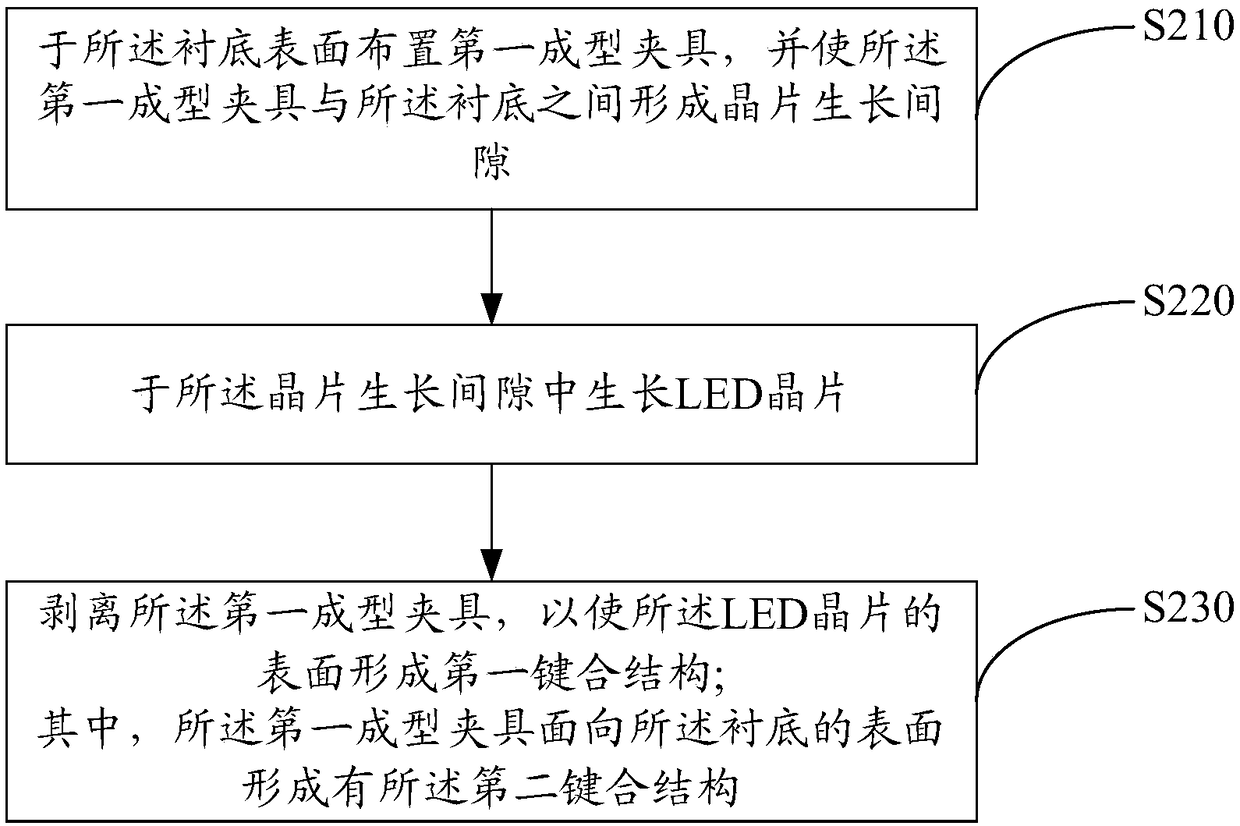
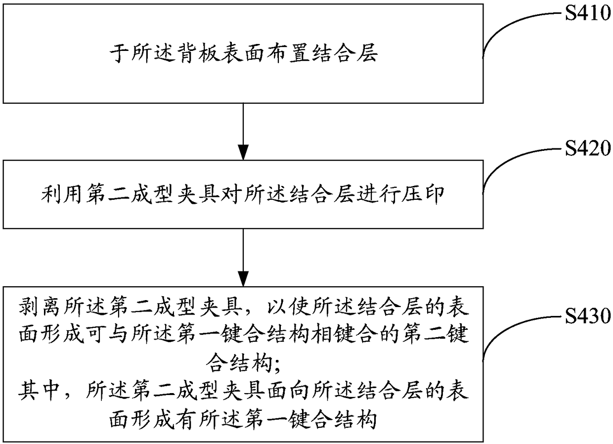
[0036] The invention provides a bonding method for LED chips.

[0037] see figure 1 , in an embodiment of the bonding method of the LED chip of the present invention, the bonding method of the LED chip comprises the following steps:

[0038] Step S100, providing a substrate.

[0039] Specifically, sapphire substrates can generally be selected as substrates. Sapphire substrates have many advantages: first, the production technology of sapphire substrates is mature and the quality is good; second, sapphire substrates have good st...


PUM


Abstract

The invention discloses an LED wafer bonding method. The LED wafer bonding method comprises the following steps that a substrate is provided; an LED wafer is grown on the surface of the substrate, anda first bonding structure is enabled to be formed on the surface of the LED wafer; a backboard is provided; a binding layer is arranged on the surface of the backboard, and a second bonding structurecapable of being bonded with the first bonding structure is formed on the surface of the binding layer; and the LED wafer is aligned with the binding layer, and the first bonding structure and the second bonding structure are enabled to be bonded. The utilization rate of the backboard can be enhanced by the technical scheme.

Description

technical field [0001] The invention relates to the technical field of LEDs, in particular to a method for bonding LED chips. Background technique [0002] With the development and progress of technology, Micro LED has shown many advantages over OLED. For example, the LED chip of Micro LED is smaller and has a longer life, and Micro LED is far superior to OLED in terms of module thickness, power consumption, brightness, screen response time, resolution, and display effect. Therefore, MicroLED is a very competitive technology. However, in the manufacturing process of Micro LED, there is a problem of accurately positioning the LED chip on the backplane. At present, in order to solve such a difficult problem, a common practice is to provide alignment marks on the backplane and the substrate, so as to realize precise positioning by using the alignment marks. However, when such an approach is adopted, the alignment marks occupy valuable space on the backplane, resulting in low...

Claims


Application Information

Patent Timeline
Patent Type & Authority Applications(China)
IPC IPC(8): H01L21/60H01L21/68H01L33/00
CPCH01L21/68H01L24/02H01L24/03H01L33/005H01L2224/03015
Inventor 牛小龙徐相英姜晓飞
Owner GOERTEK INC
Why Eureka
Try Eureka