SRAM memory and formation method
A memory and latch technology, applied in the direction of electric solid state devices, semiconductor devices, electrical components, etc., can solve problems such as poor electrical performance of static random access memory, and achieve the effect of improving speed
- Summary
- Abstract
- Description
- Claims
- Application Information
AI Technical Summary
Problems solved by technology
Method used
Image

Examples
Embodiment Construction
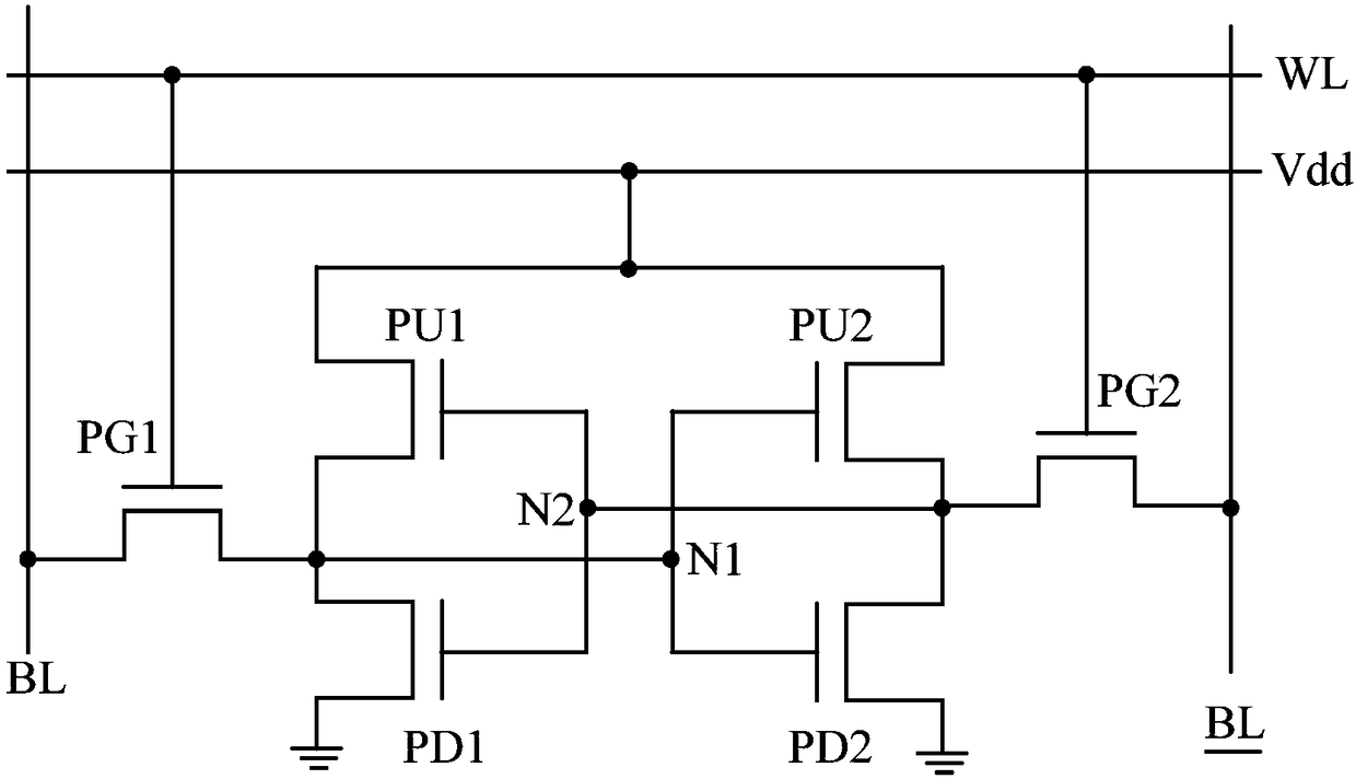
[0032] As mentioned in the background, the electrical performance of the SRAM memory formed in the prior art is relatively poor.
[0033] figure 1 It is a circuit diagram of a SRAM memory unit, the SRAM memory unit includes a pass transistor, a pull-up transistor and a pull-down transistor, the pass transistor includes: a first pass transistor PG1 and a second pass transistor PG2, and the pull-up transistor includes a first A pull-up transistor PU1 and a second pull-up transistor PU2. The pull-down transistor includes a first pull-down transistor PD1 and a second pull-down transistor PD2. The pull-up transistor and the pull-down transistor form a latch. For the connection relationship of the transfer transistor, pull-up transistor and pull-down transistor, refer to figure 1 .
[0034]When reading data "0", the current in PD1 must be greater than the current in PG1, otherwise the data "0" cannot be read correctly; when writing data "0", the current in PG1 must be greater than...
PUM
 Abstract
Description
Claims
Application Information
 - R&D
- Intellectual Property
- Life Sciences
- Materials
- Tech Scout
- Unparalleled Data Quality
- Higher Quality Content
- 60% Fewer Hallucinations
Browse by: Latest US Patents, China's latest patents, Technical Efficacy Thesaurus, Application Domain, Technology Topic, Popular Technical Reports.
© 2025 PatSnap. All rights reserved.Legal|Privacy policy|Modern Slavery Act Transparency Statement|Sitemap|About US| Contact US: help@patsnap.com