Image sensor and formation method thereof

A technology of image sensor and interlayer dielectric layer, which is applied in the manufacture of electric solid-state devices, semiconductor devices, semiconductor/solid-state devices, etc. It can solve the problems that the size of the metal grid is not easy to control, etc., so as to ensure performance, save costs and reduce usage. Reduced effect

Inactive Publication Date: 2018-08-31
HUAIAN IMAGING DEVICE MFGR CORP
View PDF1 Cites 7 Cited by
  • Summary
  • Abstract
  • Description
  • Claims
  • Application Information

AI Technical Summary

Problems solved by technology

[0005] However, with the continuous reduction of process nodes, the size of the metal grid is becoming more and more difficult to control in the process of manufacturing back-illuminated image sensors.

Method used


Image

  • Image sensor and formation method thereof
  • Image sensor and formation method thereof
  • Image sensor and formation method thereof

Examples


no. 1 example

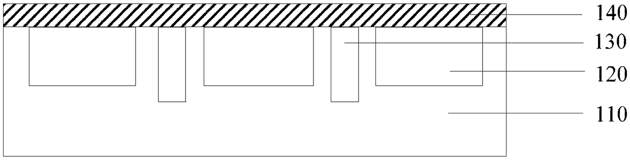
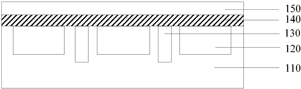
[0030] Figure 2 to Figure 9 It is a structural diagram corresponding to each step of the method for forming the back-illuminated image sensor in the first embodiment of the present invention.

[0031] refer to figure 2 , providing a semiconductor substrate 110, forming a discrete photodiode 120 in the semiconductor substrate 110; forming a deep trench isolation structure 130 in the semiconductor substrate 110, and the deep trench isolation structure 130 is located at the photodiode 120 between, and the depth of the deep trench isolation structure 130 is deeper than that of the photodiode 120, so as to obtain a better isolation effect and avoid the problem of photo-generated carrier diffusion between different pixel regions; in the semiconductor An interlayer dielectric layer 140 is formed on the surface of the substrate 110 , and the interlayer dielectric layer 140 covers the photodiode 120 and the deep trench isolation structure 130 .

[0032] In this embodiment, the semi...

no. 2 example

[0058] Figure 10 to Figure 18 It is a structural diagram corresponding to each step of the method for forming a back-illuminated image sensor in the second embodiment of the present invention.

[0059] refer to Figure 10 , providing a semiconductor substrate 210, forming a discrete photodiode 220 in the semiconductor substrate 210; forming a deep trench isolation structure 230 in the semiconductor substrate 210, and the deep trench isolation structure 230 is located at the photodiode 220 between, and the depth of the deep trench isolation structure 230 is deeper than that of the photodiode 220, so as to obtain a better isolation effect and avoid the problem of photo-generated carrier diffusion between different pixel regions; in the semiconductor An interlayer dielectric layer 240 is formed on the surface of the substrate 210 , and the interlayer dielectric layer 240 covers the photodiode 220 and the deep trench isolation structure 230 .

[0060] In this embodiment, the ma...


PUM


Abstract

The technical scheme discloses an image sensor and a formation method thereof; the image sensor forming method comprises the following steps: providing a semiconductor substrate; forming a discrete photodiode and a deep trench isolation structure in the semiconductor substrate, wherein the deep trench isolation structure is located between the photodiode; forming an interlayer dielectric layer onthe surface of the semiconductor substrate so as to cover the photodiode and the deep trench isolation structure; forming an amorphous form carbon layer on the interlayer dielectric layer; etching theamorphous form carbon layer so as to expose the interlayer dielectric layer surface, thus forming a groove; forming an insulation layer on the surface of the amorphous form carbon layer, and the sidewalls and the bottom of the groove; forming a metal layer on the surface of the insulation layer; etching the metal layer and the insulation layer so as to expose the interlayer dielectric layer surface, thus forming discrete metal grids; removing the amorphous form carbon layer. When the key dimensions of the formed metal grids are small enough, collapse conditions cannot happen.

Description

technical field [0001] The invention relates to the manufacturing field of semiconductor devices, in particular to an image sensor and its forming method, especially a back-illuminated image sensor and its forming method. Background technique [0002] An image sensor receives light signals from an object and converts the light signals into electrical signals, which can then be transmitted for further processing, such as digitization, and then stored in a storage device such as a memory, optical or magnetic disk, or used in a display display, print, etc. Image sensors are commonly used in devices such as digital cameras, video cameras, scanners, facsimile machines, and the like. [0003] Image sensors are generally of two types, Charge Coupled Device (CCD) sensors and CMOS Image Sensors (CIS). CCD is called a photocoupler device, which collects charge through the photoelectric effect, and the charge of each row of pixels is sent to the analog shift register with the clock s...

Claims


Application Information

Patent Timeline
Patent Type & Authority Applications(China)
IPC IPC(8): H01L27/146H01L21/20
CPCH01L27/14601H01L21/20H01L27/14683
Inventor 穆钰平黄晓橹周艮梅
Owner HUAIAN IMAGING DEVICE MFGR CORP
Why Eureka
Try Eureka