Organic light emitting diode (OLED) substrate and display device

A substrate and display area technology, which is applied in the manufacture of electrical components, electrical solid-state devices, semiconductor/solid-state devices, etc., can solve the problems of easy breakage of the encapsulation layer, deterioration of the function of OLED devices, and damage.

Active Publication Date: 2018-09-04
BOE TECH GRP CO LTD
View PDF3 Cites 3 Cited by
  • Summary
  • Abstract
  • Description
  • Claims
  • Application Information

AI Technical Summary

Problems solved by technology

[0005] In the flexible process, OLED devices are generally manufactured on a flexible substrate, and an encapsulation layer is prepared on the OLED device to seal the OLED device and prevent contamination by impurities such as water and oxygen. However, when bending frequently, the bending area is due to Affected by the stress on both sides of the OLED device, the encapsulation layer of the OLED device is easier to break, resulting in deterioration or even damage to the function of the OLED device
After the function of the OLED device deteriorates, the display effect and product life will be greatly affected

Method used


Image

  • Organic light emitting diode (OLED) substrate and display device
  • Organic light emitting diode (OLED) substrate and display device
  • Organic light emitting diode (OLED) substrate and display device

Examples


Embodiment 1

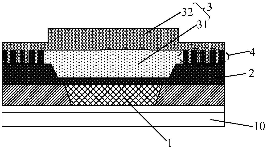
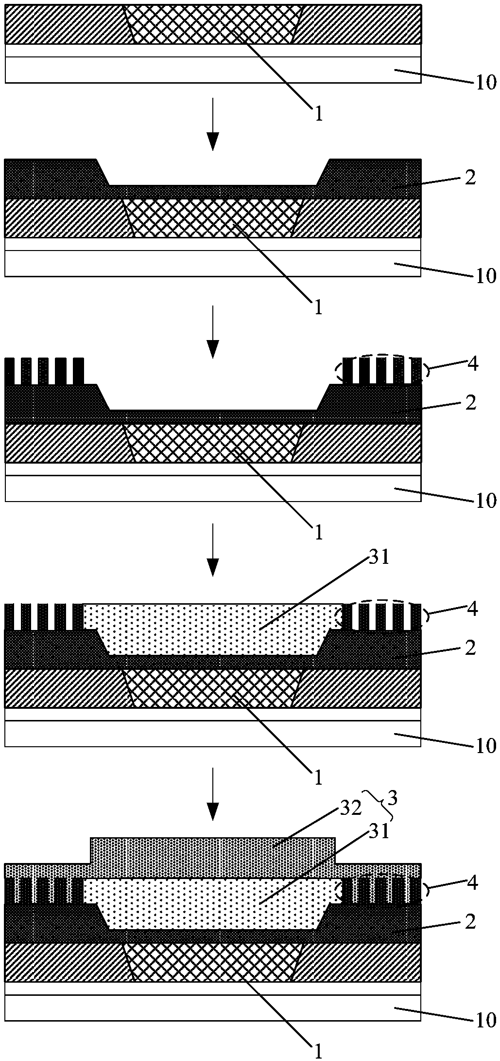
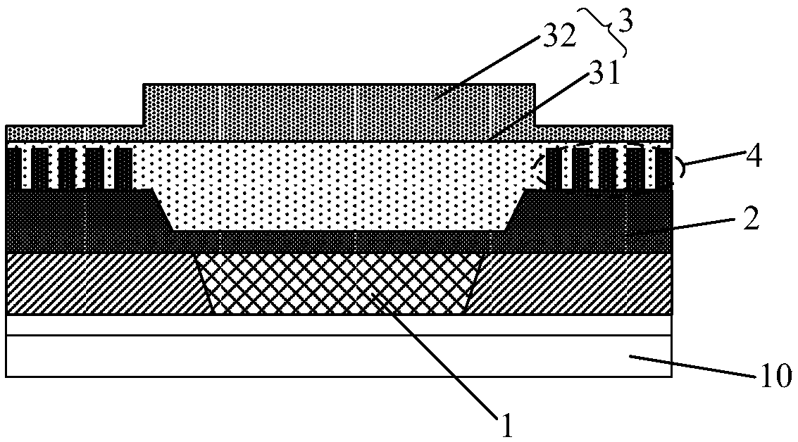
[0033] combine figure 1 , 3 , 4, and 5, the present embodiment provides a flexible OLED substrate, which has a plurality of display areas and non-display areas surrounding the display areas; wherein, the OLED substrate includes a flexible base 10, which is arranged on the flexible base 10 and is connected to the flexible base 10. The OLED device 1 corresponding to the position of the display area; the encapsulation layer located above the OLED device 1; wherein, the encapsulation layer includes: a pre-encapsulation layer 2 disposed above the layer where the OLED device 1 is located, and a protective layer 3 disposed above the pre-encapsulation layer 2; In particular, a buffer layer 4 is disposed in the protective layer 3 at a position corresponding to a part of the non-display area, and the toughness of the buffer layer 4 is greater than that of the protective layer 3 .

[0034] It should be noted here that the bending area of ​​the flexible substrate is usually located in th...

Embodiment 2

[0052] This embodiment provides a display device, including the OLED substrate provided in Embodiment 1.

[0053] Since the display device in this embodiment includes the OLED substrate in Embodiment 1, its bending resistance is better.

[0054] Wherein, the display device may be an OLED display device, such as electronic paper, OLED panel, mobile phone, tablet computer, television, monitor, notebook computer, digital photo frame, navigator and any other product or component with display function.


PUM


Abstract

The invention provides an organic light emitting diode (OLED) substrate and a display device, and belongs to the technical field of display. By the OLED substrate and the display device, the problem that a package layer of a traditional flexible OLED substrate is easy to break can be solved. The OLED substrate is provided with a plurality of display regions and non-display regions, wherein the display regions are encircled by the non-display regions, the OLED substrate comprises a flexible substrate, OLED devices, a pre-package layer and a protection layer, the OLED devices are arranged on theflexible substrate and are corresponding to positions of the display regions, the pre-package layer is arranged on a layer where the OLED devices are located, the protection layer is arranged on thepre-package layer, buffer layers are arranged at positions, corresponding to at least one part of the non-display regions, in the protection layer, and the flexibility of the buffer layers is larger than the flexibility of the protection layer.

Description

technical field [0001] The invention belongs to the field of display technology, and in particular relates to an OLED substrate and a display device. Background technique [0002] An organic light emitting diode (Organic Light Emitting Diode, referred to as: OLED) has the characteristic of self-luminescence, and when a current passes through it, the OLED will emit light. With the rapid progress of display technology, semiconductor element technology, which is the core of the display device, has also been greatly improved. For existing display devices, organic light-emitting diodes, as a current-mode light-emitting device, are increasingly being used because of their characteristics such as self-illumination, fast response, wide viewing angle, and the ability to be fabricated on flexible substrates. It is used in the field of high-performance display. [0003] Organic Electroluminescent Display (Organic Electroluminescent Display), with its low power consumption, high color...

Claims


Application Information

Patent Timeline
Patent Type & Authority Applications(China)
IPC IPC(8): H01L51/52
CPCH10K50/844
Inventor 田宏伟牛亚男刘政赵梦左岳平王雷
Owner BOE TECH GRP CO LTD
Why Eureka
Try Eureka