Clock-controlled D flip-flop based on FinFET device

A trigger and device technology, applied in electrical components, electrical pulse generator circuits, pulse generation, etc., can solve the problems of large power consumption delay product, large power consumption, large area, etc.

Inactive Publication Date: 2018-09-04
NINGBO UNIV
View PDF4 Cites 0 Cited by
  • Summary
  • Abstract
  • Description
  • Claims
  • Application Information

AI Technical Summary

Problems solved by technology

In the clocked D flip-flop, the internal structure of each two-input NAND gate in the master latch and the slave latch includes at least four Fin Field-Effect Transistors (Fin Field-Effect Transistors), The fin field effect transistor contained in each two-input NAND gate is in the common gate (Common Multi-Gate) working mode. Therefore, although the overall structure of the clocked D flip-flop is relatively simple, all the components in the overall structure The number of consumed FinFET tubes is large, the area is large, there will be large power consumption, and the power consumption delay product is also large, which is not conducive to the design of low-power circuits

Method used


Image

  • Clock-controlled D flip-flop based on FinFET device
  • Clock-controlled D flip-flop based on FinFET device
  • Clock-controlled D flip-flop based on FinFET device

Examples


Embodiment 1

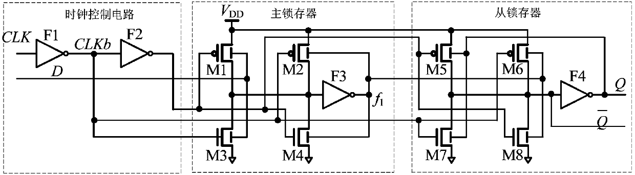
[0015] Embodiment one: if figure 2 As shown, a clocked D flip-flop based on a FinFET device includes a master latch and a slave latch. The clocked D flip-flop also includes a clock control circuit, and the clock control circuit includes a first inverter F1 and a second inverter F1. Inverter F2, the input terminal of the first inverter F1 is the clock input terminal of the clock control circuit for accessing the clock signal CLK, the output terminal of the first inverter F1 and the input terminal of the second inverter F2 connected and its connection end is the inverting clock output end of the clock control circuit, the inversion signal CLKb of the output clock signal CLK, the output end of the second inverter F2 is the clock output end of the clock control circuit; the main latch includes the first A FinFET tube M1, a second FinFET tube M2, a third FinFET tube M3, a fourth FinFET tube M4 and a third inverter F3, the first FinFET tube M1 and the second FinFET tube M2 are P-ty...

Embodiment 2

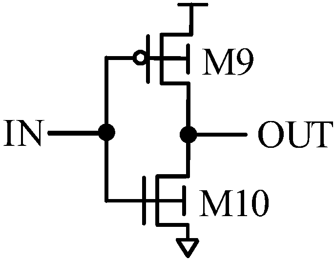
[0016] Embodiment 2: This embodiment is basically the same as Embodiment 1, the only difference is that in this embodiment, the first inverter F1 includes a ninth FinFET tube M9 and a tenth FinFET tube M10, and the ninth FinFET tube M9 is a P-type FinFET The tenth FinFET tube M10 is an N-type FinFET tube, the number of fins in the ninth FinFET tube M9 is 2, and the number of fins in the tenth FinFET tube M10 is 1; the source of the ninth FinFET tube M9 is connected to the power supply VDD, and the ninth FinFET tube M9 has The front gate of the FinFET tube M9, the back gate of the ninth FinFET tube M9, the front gate of the tenth FinFET tube M10, and the back gate of the tenth FinFET tube M10 are connected, and the connection terminal is the input terminal of the first inverter F1, and the connection terminal of the tenth FinFET tube M10 is connected to the input terminal of the first inverter F1. The drain of the ninth FinFET tube M9 is connected to the drain of the tenth FinFE...


PUM


Abstract

The invention discloses a clock-controlled D flip-flop based on a FinFET device. The clock-controlled D flip-flop comprises a master latch and a slave latch, and the clock-controlled D flip-flop further comprises a clock control circuit, wherein the clock control circuit comprises a first inverter and a second inverter, the master latch comprises a first FinFET transistor, a second FinFET transistor, a third FinFET transistor, a fourth FinFET transistor and a third inverter, the slave latch comprises a fifth FinFET transistor, a sixth FinFET transistor, a seventh FinFET transistor, an eighth FinFET transistor and a fourth inverter, and the fifth FinFET transistor and the sixth FinFET transistor are both P-type FinFET transistors. Thereby, the scheme of the invention has the advantage thatin the case of not affecting the circuit performance, the circuit area, power consumption and power consumption-time delay product are all small.

Description

technical field [0001] The invention relates to a clocked D flip-flop, in particular to a clocked D flip-flop based on a FinFET device. Background technique [0002] In the field of digital electronic technology, sequential logic circuits are composed of storage circuits and combinational logic, and storage components are used to maintain the logic state of sequential logic circuits. As a storage circuit, flip-flop is one of the basic circuits of digital circuits and plays an important role in digital circuit systems. [0003] With the continuous advancement of VISL technology, in the digital circuit system that does not require high operating speed, its power consumption requirements continue to increase, and the requirements for flip-flop performance are also more stringent. It is required that the flip-flop should have both low power consumption and low power consumption. Time-consuming delay product. The performance of the flip-flop's power consumption, power consumpti...

Claims


Application Information

Patent Timeline
Patent Type & Authority Applications(China)
IPC IPC(8): H03K3/012H03K3/027
CPCH03K3/012H03K3/027
Inventor 胡建平朱昊天张鹏烽
Owner NINGBO UNIV
Why Eureka
Try Eureka