Preparation method of array substrate and preparation method of distance piece structures thereof

A technology of array substrate and light-transmitting structure, which is applied in the photoplate making process of the patterned surface, electrical components, semiconductor devices, etc., can solve the problems that the surface is not flat enough, affects the yield rate, etc., and achieves the effect of reducing the height and increasing the step difference

Active Publication Date: 2018-09-07
SHENZHEN CHINA STAR OPTOELECTRONICS SEMICON DISPLAY TECH CO LTD
View PDF3 Cites 2 Cited by
  • Summary
  • Abstract
  • Description
  • Claims
  • Application Information

AI Technical Summary

Problems solved by technology

[0004] The final level difference between the main spacer 140' and the secondary spacer 141' will affect the safe range of the liquid crystal limit (LCMargin) in the cell manufacturing process, thereby affecting the yield rate. In many existing applications, you will face such a level difference too small problem; meanwhile, in the prior art, the surface of the sub-spacer 141' is not flat enough

Method used


Image

  • Preparation method of array substrate and preparation method of distance piece structures thereof
  • Preparation method of array substrate and preparation method of distance piece structures thereof
  • Preparation method of array substrate and preparation method of distance piece structures thereof

Examples


Embodiment Construction

[0045] The following will clearly and completely describe the technical solutions in the embodiments of the present invention with reference to the accompanying drawings in the embodiments of the present invention. Obviously, the described embodiments are only part of the embodiments of the present invention, not all of them. Based on the embodiments of the present invention, all other embodiments obtained by persons of ordinary skill in the art without making creative efforts belong to the protection scope of the present invention.

[0046] Here, it should also be noted that, in order to avoid obscuring the present invention due to unnecessary details, only the structures and / or processing steps closely related to the solution according to the present invention are shown in the drawings, and the related Other details are not relevant to the invention.

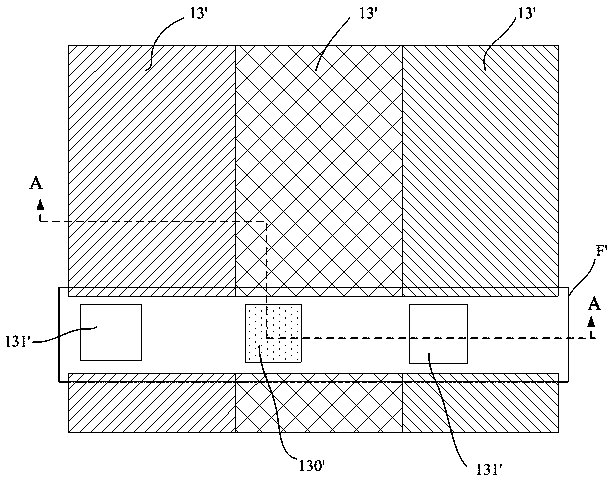
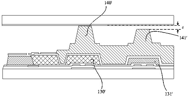
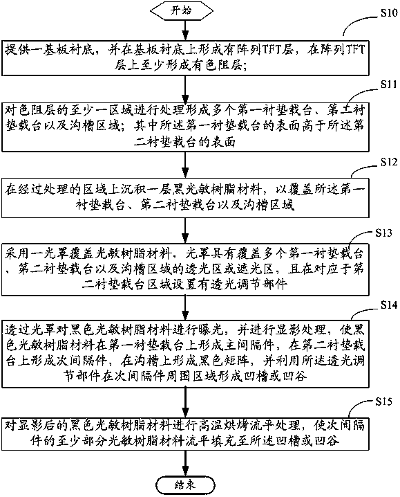
[0047] Such as image 3 As shown, it shows a schematic diagram of the main process of an embodiment of a method for prepari...


PUM


Abstract

The embodiment of the invention discloses a preparation method of distance piece structures of an array substrate. The preparation method comprises the following steps: forming a plurality of first gasket carrying tables and second gasket carrying tables with different heights on a color resistance layer of the array substrate; depositing a black photosensitive resin material layer with which thefirst gasket carrying tables and the second gasket carrying tables are on the array substrate; carrying out exposure on the photosensitive resin material through a light-transmitting photomask provided with a light-transmitting area or a light-shading area, enabling the area of the second gasket carrying tables to be provided with a light-transmitting adjusting component, carrying out developing treatment, forming main distance pieces on the first gasket carrying tables by using the black photosensitive resin material, forming secondary distance pieces on the second gasket carrying tables, andforming grooves or trenches in the peripheral regions of the secondary distance pieces; carrying out high temperature baking leveling treatment on the developed black photosensitive resin material sothat at least a part of the black photosensitive resin material of the secondary distance pieces is leveled out and filled into the grooves or trenches. The invention also discloses a preparation method of the corresponding array substrate. Through the embodiment of the invention, the segment gaps between the main distance pieces and the secondary distance pieces can be increased, the flatness isimproved, and the product yield can be improved.

Description

technical field [0001] The invention relates to the display field, in particular to a method for preparing an array substrate and a method for preparing a spacer structure. Background technique [0002] BPS (Black Photo Spacer, black spacer) technology is to integrate two independent processes of BM ((Black Matrix, black matrix) and PS (Photo Spacer, spacer) in conventional liquid crystal display LCD into one, and use black light-shielding photosensitive resin to form Three functional structures with different heights, from the height to the bottom, are the main spacer (Main PS), the sub-spacer (Sub PS) and the black matrix. [0003] Such as figure 1 and figure 2 Shown is a schematic structural diagram of an existing liquid crystal display manufactured using BPS technology. Wherein, by digging out the color resist layer 13' in the grid line area (see figure 1 F' area in), and then use black light-shielding photosensitive resin to cover and make the main spacer 140' and ...

Claims


Application Information

Patent Timeline
Patent Type & Authority Applications(China)
IPC IPC(8): H01L27/12H01L21/77G03F7/00G02F1/1339
CPCH01L27/1248H01L27/1288G02F1/13394G03F7/0035G03F7/0007G02F1/13396
Inventor 曹武
Owner SHENZHEN CHINA STAR OPTOELECTRONICS SEMICON DISPLAY TECH CO LTD
Why Eureka
Try Eureka