Welding structure and semiconductor part

A technology for welding structures and semiconductors, which is applied in semiconductor devices, semiconductor/solid-state device components, electric solid-state devices, etc., and can solve problems such as poor welding quality

Inactive Publication Date: 2018-09-11
KONFOONG MATERIALS INTERNATIONAL CO LTD
View PDF11 Cites 3 Cited by
  • Summary
  • Abstract
  • Description
  • Claims
  • Application Information

AI Technical Summary

Problems solved by technology

[0005] The purpose of the present invention is to provide a welded structure to solve the technical pr

Method used


Image

  • Welding structure and semiconductor part
  • Welding structure and semiconductor part
  • Welding structure and semiconductor part

Examples


Embodiment 1

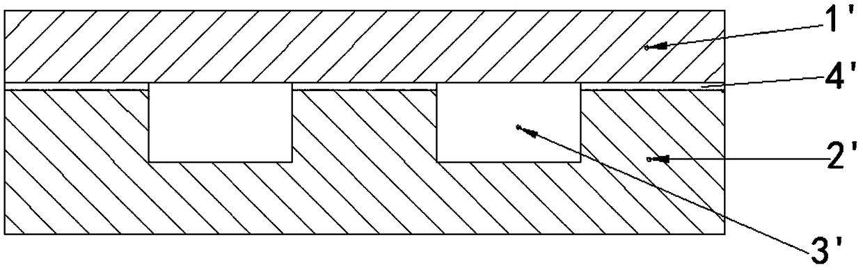
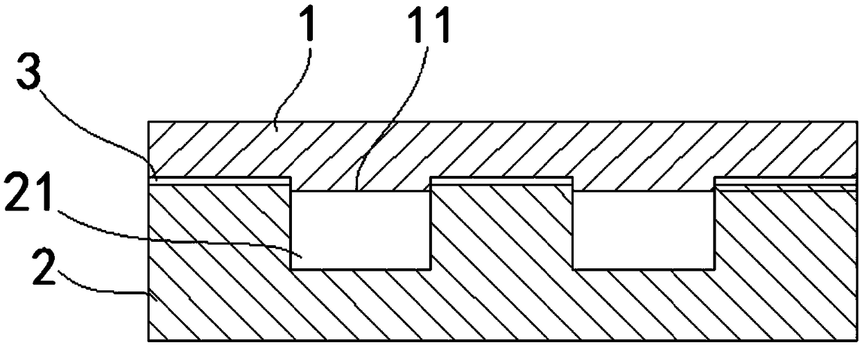
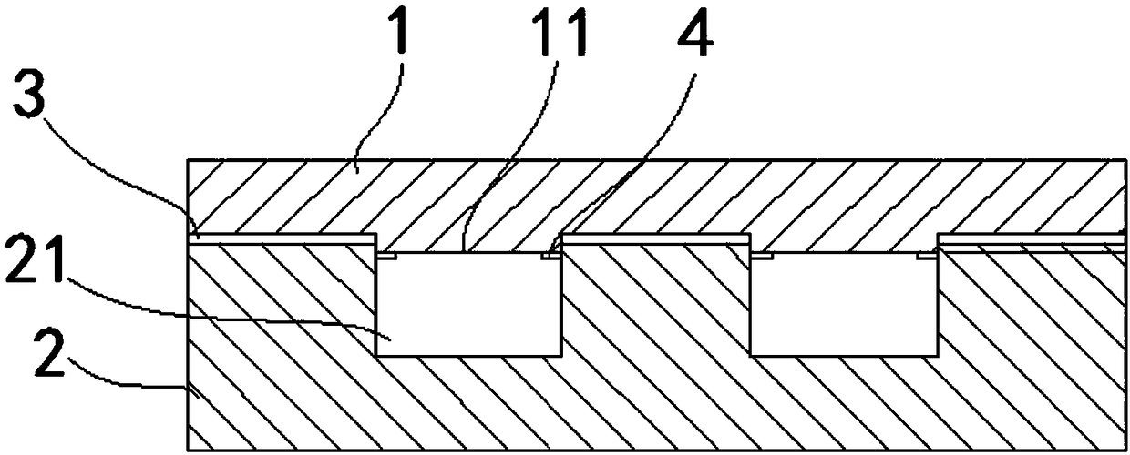
[0030] The welded structure provided by this embodiment, such as Figure 2 to Figure 3 As shown, it includes a cover plate 1 and a bottom plate 2; Through the arrangement, the groove 21 forms an opening with the first end surface; the cover plate 1 has a second end surface, the first end surface is opposite to the second end surface, and the second end surface is provided with a convex 11, the protrusion 11 can close the opening, and there is a gap between the first end surface and the second end surface, the gap is used to set the solder layer 3, the cover plate 1 and the bottom plate 2 soldered through said solder layer 3.

[0031] When welding the cover plate 1 and the bottom plate 2, the solder layer 3 is heated, the pressure is applied to the cover plate 1 toward the bottom plate 2, and the pressure is applied to the bottom plate 2 toward the cover plate 1, so that the two are welded together. The protrusion 11 and the groove 21 can form a channel. Since the protrusion...

Embodiment 2

[0049] The semiconductor component provided in this embodiment includes the soldering structure described in Embodiment 1.

[0050] The welding structure includes a cover plate 1 and a bottom plate 2; the bottom plate 2 has a first end surface, a groove 21 is provided on the first end surface, and the two ends of the groove 21 are respectively connected to the side walls of the bottom plate 2 Through the arrangement, the groove 21 forms an opening with the first end surface; the cover plate 1 has a second end surface, the first end surface is opposite to the second end surface, and the second end surface is provided with a convex 11, the protrusion 11 can close the opening, and there is a gap between the first end surface and the second end surface, the gap is used to set the solder layer 3, the cover plate 1 and the bottom plate 2 soldered through said solder layer 3.

[0051] When welding the cover plate 1 and the bottom plate 2, the solder layer 3 is heated, the pressure i...


PUM


Abstract

The invention provides a welding structure and a semiconductor part, and relates to the technical field of semiconductor equipment. The welding structure includes a cover plate and a bottom plate; thebottom plate has a first end face, grooves are arranged in the first end face, and two ends of the grooves penetrate through a side wall of the bottom plate, and the grooves and the first end face form openings; and the cover plate has a second end face, the first end face is arranged opposite to the second end face, the second end face is provided with bulges, the bulges can seal the openings, and a gap between the first end face and the second end face is provided for arrangement of a solder layer, and the cover plate and the bottom plate are welded through the solder layer. When the coverplate and bottom plate are welded, the solder layer is heated, pressure towards the bottom plate is applied to the cover plate , pressure towards the cover plate is applied to the bottom plate, sincethe bulges can seal the openings, the solder layer in the gap is prevented from flowing into the grooves, the solder between the cover plate and the bottom plate is prevented from being insufficient,the probability of poor welding is reduced, the blockage of a water channel or an air passage can also be prevented, and the welding quality of the welding structure is improved.

Description

technical field [0001] The invention relates to the technical field of semiconductor equipment, in particular to a welding structure and a semiconductor part with the welding structure. Background technique [0002] A semiconductor refers to a material whose conductivity at room temperature is between that of a conductor and an insulator. Semiconductors have a wide range of applications in radios, televisions, and temperature measurement. For example, diodes are parts made of semiconductors. The core units of most electronic products, such as computers, mobile phones or digital recorders, are closely related to semiconductors. Common semiconductor materials are silicon, germanium, gallium arsenide, etc. [0003] In semiconductor parts, water channels or air channels are often required to allow liquid or gas to flow in the water channels or air channels. In the existing technology, such as figure 1 As shown, a semiconductor part with a water channel or an air channel is ...

Claims


Application Information

Patent Timeline
IPC IPC(8): H01L23/10
Inventor 姚力军潘杰王学泽周建军
Owner KONFOONG MATERIALS INTERNATIONAL CO LTD
Why Eureka
Try Eureka