Low-dark-count-rate CMOS SPAD photoelectric device

An optoelectronic device and counting rate technology, applied in the field of single-photon detection, can solve the problems of low dark count rate, high fill factor and high photon detection efficiency, and achieve the goal of reducing dark current, reducing dark count rate, and avoiding edge breakdown. Effect

Active Publication Date: 2018-09-18
CHONGQING UNIV OF POSTS & TELECOMM
View PDF5 Cites 8 Cited by
  • Summary
  • Abstract
  • Description
  • Claims
  • Application Information

AI Technical Summary

Problems solved by technology

Simple scaling down of the traditional SPAD device structure cannot achieve a low ...

Method used


Image

  • Low-dark-count-rate CMOS SPAD photoelectric device
  • Low-dark-count-rate CMOS SPAD photoelectric device
  • Low-dark-count-rate CMOS SPAD photoelectric device

Examples


Embodiment Construction

[0022] The technical solutions in the embodiments of the present invention will be described clearly and in detail below with reference to the drawings in the embodiments of the present invention. The described embodiments are only some of the embodiments of the invention.

[0023] The technical scheme that the present invention solves the problems of the technologies described above is:

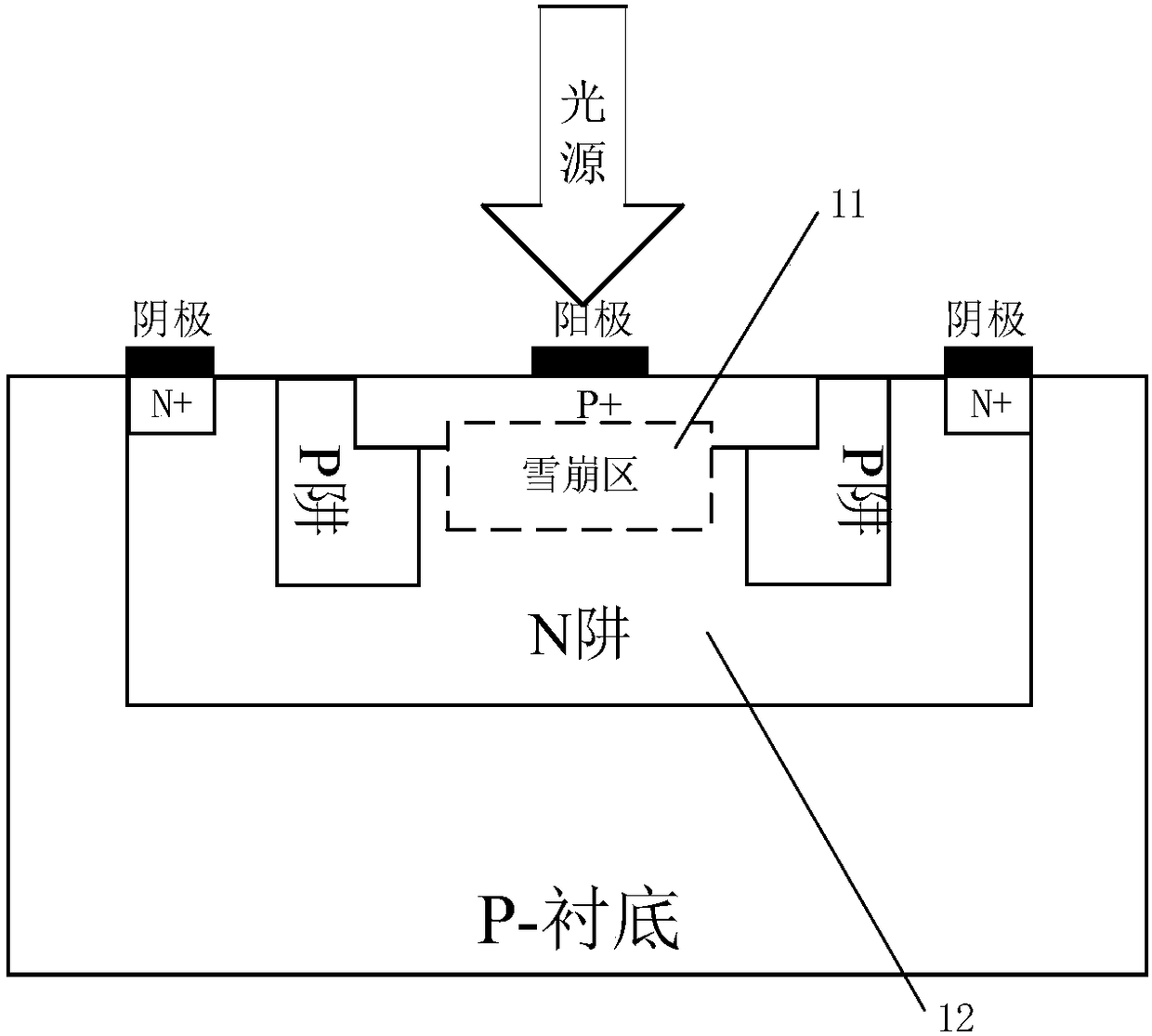
[0024] Such as figure 1 Shown is a structural diagram of a conventional CMOS SPAD optoelectronic device. It can be seen from the figure that in this structure, the PN junction is composed of a heavily doped P-type region and a lightly doped N well. The light absorption area (corresponding to the 12 area in the figure). The P wells on both sides of the PN junction act as a guard ring to prevent premature edge breakdown of the device. The working principle of the SPAD optoelectronic device is that when the incident light enters the device and is absorbed by the light absorption region (cor...


PUM


Abstract

The invention provides a low-dark-count-rate CMOS SPAD photoelectric device. A P-well layer is added based on a routine P+/N-well type SPAD structure. The P-well layer is arranged between the P+ layerand the N-well layer. Furthermore, an N-well clearance is utilized as a virtual protecting ring of the structure; namely N-wells are added at two sides of a PN junction, wherein the structure is shown in the attached figures of an abstract. An incident photon is incident into the device and is attracted at the central N well, and furthermore a photon-generated carrier is generated. The P-well layer and the N-well layer are utilized at two sides of the PN junction. Hereon an avalanche junction is a P-well/N-well junction. Because the avalanche junction is a lightly doped avalanche junction, width of a depletion region increases, and probability of interband tunneling of the carries is reduced, thereby reducing the dark counting rate. Furthermore the virtual protecting ring is used for suppressing edge breakdown of the PN junction. The forming principle of virtual protection is characterized in that transverse diffusion exists between adjacent N-wells and therefore the N- virtual protecting ring is formed at the PN junction. The low-dark-count-rate CMOS SPAD photoelectric device is designed at two aspects of the protecting ring and the depletion region width, dark current of the device is reduced, thereby reducing the dark count rate.

Description

technical field [0001] The invention belongs to the technical field of single photon detection, relates to the structural design of an APD photoelectric device, in particular to the design of a CMOS SPAD photoelectric device with a new structure and low dark count rate. Background technique [0002] Single Photon Avalanche Diode (Single Photon Avalanche Diode), also known as SPAD, is an avalanche photodiode (Avalanche Photodiode) working in Geiger mode (working voltage greater than breakdown voltage). Since SPAD works in Geiger mode and can detect a single photon, the device has great application prospects in quantum communication technology, fluorescence lifetime imaging, three-dimensional imaging technology and other fields. [0003] The device structure of CMOS SPAD can be divided into two categories according to the type of its guard ring. One is a diffused guard ring structure, that is, a lightly doped N-well or P-well is used at the edge of the PN junction. The dark c...

Claims


Application Information

Patent Timeline
IPC IPC(8): H01L27/144H01L31/0352
CPCH01L27/1443H01L31/035272
Inventor 王巍王广陈婷曾虹谙王冠宇唐政维
Owner CHONGQING UNIV OF POSTS & TELECOMM
Why Eureka
Try Eureka